![]()
A "Software Defined Radio" or SDR consists of a transmit path and a receive path with a common digital signal processing interface. Unlike a traditional radio, a SDR uses digital signal processing to process signals as opposed to specific hardware. The SDR transmitter concept seeks to "move the digital to analog" processing as close to the antenna port as possible, leaving any associated hardware as fulfilling a "transport function" (or other supporting roles such as power supply reticulation) as opposed to providing and signal or information contribution.
This article examines the transmit path for a SDR. The ultimate goals of a SDR receiver include,
| Arbitrary Modulation Format Encoding Capability | |
| Software Defined Signal Bandwidth and Data Rate Synthesis | |
| Minimal RF Signal Processing - Primarily DAC to Antenna connectivity and power amplification | |
| Ability to Transmit Multiple Signals | |
| Ability to Transmit Multiple Signals Of Arbitrary, unrelated and possibly Incompatible Formats and Data rates |
This philosophy would lead us to consider such a SDR transmitter to consist of an antenna connected to the output of an Digital to Analog Converter (DAC) driven from a fast digital computational engine (e.g. ASIC, FPGA). Although the practicality of this may progress as technology improves, the need to transmit high output power is inconsistent with the ambition to create energy efficient DAC's! A RF Power Amplifier (RFPA) is a fundamental component of a SDR transmitter.
Additional DAC limitations exist,
| Finite Bit Resolution - Sets an upper limit to transmit Signal To Noise Ratio (SNR) | |
| Finite Sample Rate - Also limits dynamic range, but also maximum synthesized signal bandwidth1 | |
| Alias Responses - All time sampled signals have multiple alias responses that require ancillary hardware based filtering | |
| Current consumption - High sample rate devices draw considerable power - this limits applications to small portable receivers | |
| High Cost - ADC devices at the forefront of mixed signal conversion technology come at a premium price. General purpose ADC devices can offer multiple converters in a package for less that $US 2, whilst a high performance 2 GHz ADC could cost more than $US 500. |
Note 1: Most DAC's typically use a "sample and hold" output with an associated sinc{x} response. Although some "TxDACs" can synthesis signals on a selected alias output, the majority operate in an over-sampling mode. Further, DAC distortion and spurious outputs tend to increase with higher signal frequency outputs.
So although the ultimate SDR concept represents a desirable goal, its implementation may be too problematic for many applications, especially those that don't need all its potential features.
For some people, "SDR" may refer to a product that has its main signal parameters defined in software. Such a radio may have some hardware imposed upper limits on modulation bandwidth, data rate or format capability but allow some flexibility within these constraints. The radio may also be incapable of generating multiple signals within a frequency domain "cluster" or it may be potentially capable of this but only if all transmitted signals share the same modulation format and data rate (i.e. "coherent").
Transmitters based on this "cut down" SDR functionality may reduce development overhead. The design of linear RFPA stages is more problematic for very wide band applications, and high peak to average ratios resulting from the generation of multiple carriers degrades overall RFPA D.C. supply power to RF channel power conversion efficiency.
Some of the performance limitations imposed on the DAC can be relaxed with alternative, but related architectures - as in my SDR receiver web article. We will consider three primary SDR transmitter approaches
| Direct RF Signal Synthesis "DRFSS" - Uses a high speed high bit resolution DAC to generates signals directly at the transmit frequencies | |
| Direct IF Signal Synthesis "DIFSS" - Uses a superhet frequency conversion process to shift lower frequency DAC output signals up to a higher spectral band position | |
| Direct IQ Signal Synthesis "DIQSS" - Uses a "direct conversion" Analog IQ to RF conversion process to translate IQ Baseband signals from a dual DAC up to the final spectral placement |
The DRFSS transmitter uses a single high performance DAC to generate one or many RF signals of potentially arbitrary nature. The associated digital hardware must match this DAC's input clock and data transfer rate (assumed to exceed several GHz) but the bulk of the digital signal processing can occur at lower clock rates as required for each modulated signal (multiple rate systems are not uncommon).
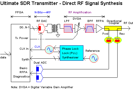
Interestingly, the technical challenges associated with a SDR transmitter reside in different areas compared to its companion SDR receiver. The actual DAC conversion technology is now well advanced as Maxim's recent announcement of their MAX5881 RF DAC with 12 Bit resolution and a sample rate as high as 4.3 GHz. Full public performance disclosure is as yet unavailable but similar advances in DAC technology can be expected by Maxim and other companies with corresponding release of detailed performance information.
Preliminary promotion data does indicate the capability to generate 4 contiguous QAM channels spaced 6 MHz apart at a center frequency of 1 GHz. The Adjacent Channel Power (ACP) at ±12 MHz offset (from band edges?) is quoted at 68 dB. Now I am guessing CATV "DOCSIS" QAM parameters for now but a QAM alpha of 0.2 would seem reasonable - higher alpha values would just be "sloppy". This implies a modulation -3 dB bandwidth of 5 MHz - i.e. a symbol rate = 5 MSymbols/s. Some inter constellation "spill-over" will occur degrading SNR unless specific measures are taken (I haven't research this application just yet - TBD) so perhaps a low level QAM16 is used - i.e. 4 bits/symbol spectral efficiency. Each QAM carrier would support a data rate of 20 MB/s under this assumption, so 4 QAM carriers would allow a data through-put of 80 MB/s (seems a bit slow - perhaps QAM256 or higher?).
(I will look into this later to see if OFDM could have been used - cable is fairly non dispersive unlike over the air propagation with multi-path distortion I guess - just thinking).
Anyway I wonder what the SNR of this DAC may be? The summation of any four signals will have a peak voltage that is 12 dB higher than the peak of each, although statistically this occurrence may be infrequent. Still the peak to average power ratio for QAM-X versions is similar; e.g. on the I channel for example, symbol values at ±1, ±3, ±5, etc. The approximate peak symbol power (without matched filtering) is equal to the square of the maximum symbol and the approximate average power equals the average over all symbols. This implies a peak to average ratio of 10 · Log10{ 32 / [ ( 12 + 32) / 2 ] = 2.6 dB (QAM64 would suggest 3.7 dB). Let's add some additional overshoot caused by I and Q digital root raised cosine filtering of about 2 dB and estimate a possible peak to average ratio for each QAM signal to be about 5 dB.
This implies that the peak QAM power per signal must be 12 dB lower than the DAC Full Scale (FS) output. Further the RMS power for each QAM signal should then be 5 dB further down. Since ACP is measured relative to the average QAM power on each QAM signal (or equivalent) the quoted ACP value of 68 dB may well represent 68 + 5 + 12 = 85 dBFS.
The maximum theoretical SNRBW for a DAC is based on bit resolution N, sample frequency Fs and measurement bandwidth BW. One estimate is,
SNRBW = 1.76 + 6.02 · N + 10 · Log10 { ½ · Fs / BW }
Given N=12 Bits, Fs = 4.3 GHz and BW ~ 5 MHz this would predict a SNR limit of 100 dBFS. The published value of 85 dBFS falls short of this prediction but this is not unreasonable; third order intermodulation products may be present, also some clock phase noise may be contributing (the ACP improves with increased offsets) or the actual digital signal source may contain numerical noise. As mentioned, all DAC's deteriorate in RF performance as their out frequency increases.
Further, RF amplification issues associated with CATV are less problematic than high power "over the air" transmission. For example, a RFPA presented with the previous example "spectrum" may be required to produce (say) 100 watts RMS per channel. The peak envelope power could be 17 dB higher, i.e. 2,000 watts. Preserving an ACP ratio of 68 dB would require a fairly good ultra linear RFPA, presumably using feed-forward technology (in comparison, Cartesian Feedback over 24 MHz composite bandwidth would be an interesting challenge). The situation applied to CATV is somewhat different - actual cable power is far lower and demands on CATV amplifier efficiency is less critical than a corresponding 2 kW PEP RFPA even just based on device cost and thermal management issues. A CATV amplifier could use "class A" with a lot of signal back-off to reduce distortion, and imply feed-forward correction as an enhancement.
A variant of the SDR DRFSS Transmitter could conceivable be combined with fiber optic communications to allow ad-hoc deployment of complete or partial radio communication infrastructure either for (military?) preparatory exercises on in actual cases of civil emergency when such services are lost. A brief proposal is here at this link UHF Optic Transfer . This scenario would require a complete arbitrary modulation format "central transmitter" that could emulate all critical lost service transmissions in parallel,
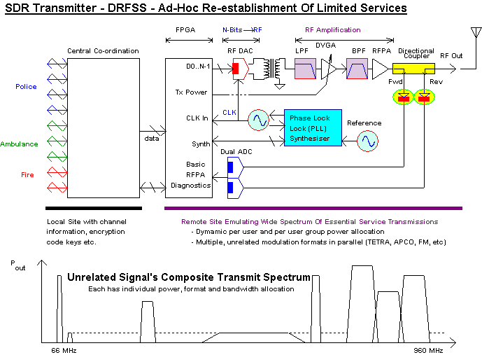
This application example is intended to indicate that current spectral regulations may be relaxed under emergency conditions - after all if an asteroid hits the earth and wipes out 99% of all radio communication then who will be concerned about transmitted "spectral purity". Similarly, training exercises required to test response capability under wide scale civil emergencies can be conducted at reduced power or by government concession so as to comply within "good neighbor" policy between spectrum users.
Other more conventional applications are still of interest. For these we may need to consider higher bit resolution DAC devices with sample rates below 1 GHz - these are far more prevalent. For example the MAX5891 DAC has a bit resolution of 16 bits with a clock sample rate of 600 MHz. This DAC and others of a similar performance would be well suited in a superhet architecture. For example, an IF frequency generated at 150 MHz could be frequency translated up to 960 MHz in a number of wide band channel steps. Finer channel steps could be generated at the IF frequency, i.e. 150 MHz ± frequency-offsets. Such a system could preserve a reasonable instantaneous transmission bandwidth and flexibility but allow low distortion and high dynamic range to be facilitated based on a lower DAC IF output frequency compared to the final RF output frequency.
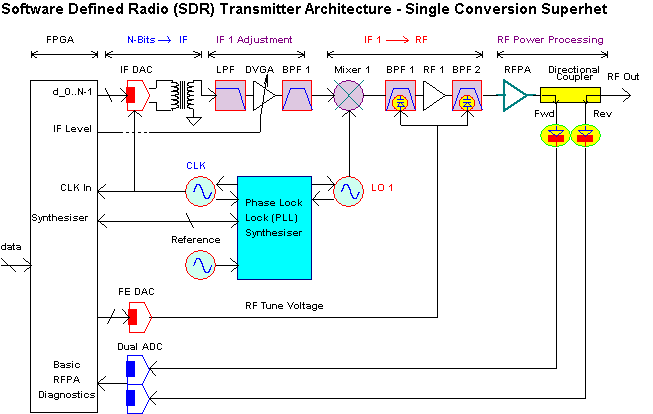
The single conversion superhet approach allows the DAC and FPGA / ASIC devices to operate at a much lower clock frequency than the Direct RF Synthesis method. For example at 500 MHz DAC may be used to produce an IF output signal at (say) 70 MHz or 140 MHz with low spurious output energy (A Band Pass filter can remove spurious energy outside the required modulation bandwidth). This IF signal can then be frequency converted to 400 - 520 MHz or 800 - 960 MHz without excessive hardware development effort. The use of electronically tuned Band Pass Filters (e.g. varicap diode tuning) makes image and LO rejection relatively straight forward and offers excellent linearity if designed appropriately.
The first IF to RF frequency conversion mixer requires some care in its selection and operating power levels. For example, it can allow harmonics of the IF input signal to appear at its RF output especially if it is over-driven. Other harmonic combinations between FIF and FLO can also produce unwanted spurious RF output energy. A high performance balanced mixer is advised (passive DBM or active IC versions). However the IF input level cannot be set too low as other unwanted spurious output mechanism with then become troublesome. These include,
| LO to RF Leakage Energy - This will be harder to filter in comparison to a weak RF output signal. Reducing the IF input drive level increases the demand on the RF Band Pass Filter in this area. | |
| Broad Band RF Output Noise - Once again, reducing the IF input drive will require additional RF amplification and this will directly increase the RF output broad band noise floor. The RF Band Pass Filters cannot be expected to significantly reject this energy due to finite "Q" and the observation that high Q varicap tuning can be in competition with varicap induced non-linearity. |
For example, lets assume the use of a conventional level 17 dBm DBM for this mixer. This may have a typical IF input 1 dB compression point P1dB of about +10 dBm and a conversion loss of 7 dB. It would probably be unwise to operate this mixer at such a high input level as spurious output generation is likely and in band distortion will be severe (QAM will be seriously compromised for example). Better spurious output rejection and modulation linearity will be achieved at IF input levels between -10 dBm and 0 dBm.
Let us assume a "rule of thumb" estimate for IIP3 given by IIP3dBm = P1dB + 10 dBm - this is a practical observation but the "10 dB" can show significant variation between device types. This example mixer may then have an input IIP3dBm = +20 dBm. It (usually) follows that,
dPdB = 2 · ( IIP3dBm - Pin, dBm )
We predict that dPdB would only be about 40 dB for Pin, dBm = 0 dBm and 60 dB for Pin, dBm = -10 dB. A high performance DAC, in comparison may achieve third order intermodulation significantly better than this limit, e.g. dB > 70 dB! It would seem like poor design practice to compromise a relatively expensive DAC performance in this area with analog induced non linearity, especially in low level processing stages. The solution may be to seek an even higher performance mixer or to further back-off its IF input drive. Let us assume a further back off of 5 dB i.e. Pin, dBm = -15 dBm for the example mixer.
The RF output level will now be 7 dB lower, i.e. -22 dBm. In comparison with typical LO to RF rejection performance associated with DBM mixers (40 ~ 50 dB), the LO leakage could be as high as -23 dBm. This is comparable to the wanted IF output and must be filtered adequately.
A typical emission limit for transmitters operating below 1 GHz is -36 dBm at the RF output (e.g. ETSI). If the required transmit output power is 100 Watts (+50 dBm) then the relative spurious emission ratio must exceed 86 dB. This high rejection ratio places some technical demands on the require band pass filter performance given that (in this example) the LO frequency may only be separated by 70 MHz or 140 MHz from the wanted RF output signal.
Now let's consider the issue of broadband noise generation in the transmitter. The output noise power from a passive DBM will be close to thermal noise, i.e. Pn, dBm = -174 dBmHz . The first RF band-pass will exhibit some loss (loss and LO + image rejection performance are in competition) and 3 dB may represent a suitable target, although perhaps optimistic. The first RF amplifier will also have an input noise contribution. If a standard MMIC "gain block" is used, a typical RF noise figure will be about NF = 3 dB. This leads to a minimum poat mixer amplifier NF = 6 dB. The corresponding input referred noise will therefore be P'n, dBm = -174 + 6 = -168 dBmHz .
The expected RF drive level, in this example, will be PRF = -22 dBm. The resulting transmit Signal to Noise Ratio "SNR" will therefore be -22 dBm - (-168 dBmHz) = 146 dBHz from this single broad band noise generating mechanism. This noise level is somewhat excessive as some Type Approval standards require SNRdB > 150 dBHz at the transmitter output!
Consequently, the superhet approach faces a dilemma. The conflict between linearity and spurious output energy (discrete or random noise) is fundamental. Device development effort continues in this area and the use of even higher IF to RF mixer performance may be essential. The use of active mixers may show worsened broad band noise due to internal amplification - however passive MOSFET based mixers (e.g. Maxim MAX and MAX ) may offer a welcome solution.
Another alternative is to reconsider the application. Operation above 1 GHz may allow relaxation on certain emission limits, also the previous emergency usage scenario may be applicable. High speed data link radios provide a suitable application for the superhet approach - either single or double conversion architectures are appropriate. These systems have lower intermodulation requirements than many PMR based applications operating below 1 GHz. Furthermore, these systems often require external, highly selective cavity tuned filters for frequency offset duplex Transmit (Tx) and Receive (Rx) operation. The use of such external filters can significantly relax the overall spurious rejection performance of the transmitter.
Operation above 1 GHz based on a dual conversion superhet approach could be conceived as follows (although note that each frequency conversion introduces additional RF broad band noise and spurious output energy)
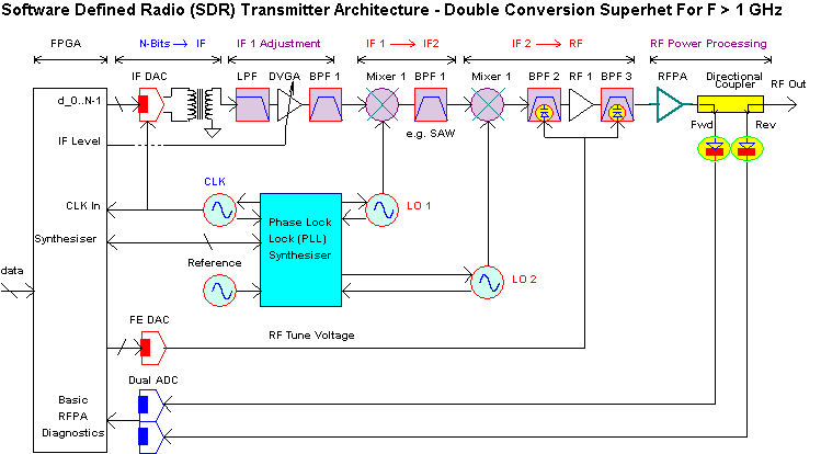
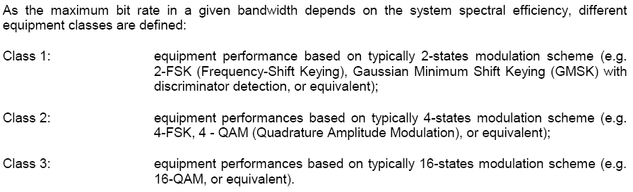
This dual conversion superhet approach may be quite appropriate for a microwave data link at 2.1 to 2.7 GHz though (e.g. ETS 300 633) and a flexible single channel bandwidth, modulation format and data rate capability would be extremely advantageous as outlined in this standard for classes 1, 2 and 3.
The Maxim MAX5881 4.3 GHz DAC would a bit "slow" for a 2.1 to 2.6 GHz DRFSS transmitter but would be excellent for IF generation in a single conversion superhet. Further, a lower speed DAC would be suitable for a double conversion superhet based transmitter as shown previously.
(Note: Microwave data link transmitters typically use class A power amplifiers with a small amount of power back-off required to meet ACP requirements - usually not overly stringent compared to PMR etc).
The final architecture is based on Analog IQ to RF modulation. This architecture is described further in my web pages at Analog IQ and Tx IQ Correction . Significant IQ performance enhancement is available when IQ error estimation and correction algorithms are incorporated in the transmitter system. These are relatively simple to implement and have low computational overhead.
Note: Direct Conversion can represent an elegant architecture with excellent performance potential. Some implementation care is required however. Two such areas to place some engineering emphasis on include,
| Non Linear Harmonic Intermodulation In The Post IQ to RF Modulator Amplifier - The 2nd and 3rd harmonic components can mix to create a new on frequency component, appearing as additional in band noise. For example, let's image the IQ to RF modulator produces a single offset tone at (say) FRF = FLO + 1 MHz. The output at 2 · FRF with be 2 · FLO ± 1 MHz (DSB). The output at 3 · FRF will be 3 · FLO - 1 MHz. The 3rd order intermodulation terms falling at FRF will now be FRF = FLO and FRF = FLO - 2 MHz - i.e. additional noise and carrier leakage that may both degrade the overall transmitted SNR. The solution is to place a simple Low Pass Filter after the IQ to RF Modulator. | |
| RF "Re-circulation" From The RFPA to the LO VCO - The VCO will be sensitive to signals feedback at or near its oscillation frequency. This will cause frequency modulation (FM) perturbations on its output. The resulting output modulation would then be corrupted, again degrading transmit SNR. The solution is two-fold; reasonable care with layout, shielding and other isolation methods should be taken. In addition, operating the VCO at a higher frequency and dividing down by 2:1 or 4:1 will result in significant improvement. |
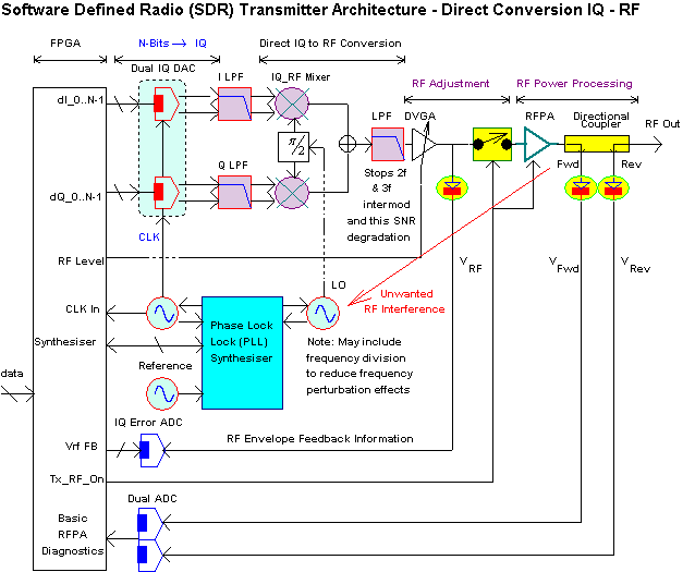
Direct Conversion IQ to RF Transmitter architecture can provide excellent performance with careful design. The DAC devices operate at the lowest possible output frequencies resulting in the best possible Spurious Free Dynamic Range (SFDR) performance. In addition, any higher frequency spurious energy, including alias output energy is easily removed with I and Q low pass filters - these may be relatively simple OpAmp based topologies. Further, significant component technology advances have been made in high dynamic range Analog IQ to RF Modulator performance. Some of these devices (e.g. passive FET MAX2021 and MAX2022 IQ to RF Modulators) have extremely high IIP3dBm linearity and essentially low broadband output noise close to the thermal limit.
Further to this, IQ error estimation and correction algorithms can further enhance in band SNR performance. In principle, QAM constellations up to QAM1024 are realistically attainable with a DIQSS architecture.
The Analog IQ to RF "DIQSS" Transmitter represents a great technology match between high performance DAC technology and IQ to RF Modulator technology. The error correction algorithms are not always available in the public domain as yet. I hope my web articles illuminate some of the potential to be gained in these areas.
We will now consider typical performance parameters for devices suitable for SDR DRFSS, DIFSS and DIQSS transmitters. This will include DAC and IQ to RF modulators at this stage.
| Manufacturer | Device Name | Bit Resolution | Sample Rate
GHz |
I3
dBFS |
SNR1Hz
dBFS @ FMHz |
SFDR
dBFS @ FMHz |
Iout
mA |
Vs
Volts |
Ps
Watts |
| Maxim | MAX5881 | 12 | 4.3 | 682 | 1731 | 68 @ 1000 | [2, 20] | [1.8, 3.3] | 1.16 |
| Maxim | MAX19692 | 12 | 2.3 | 162 @ 200 | 68 @1200 | [?, 20] | [1.8, 3.3] | 0.76 | |
| Maxim | MAX58913 | 16 | 600 | -95 @ 30
-71 @ 130 |
163 @ 36 | 80 @ 30
71 @ 130 |
[2, 20] | [1.8, 3.3] | 0.298 |
| Analog | AD9736 | 14 | 1200 | -88 @ 40
-84 @ 130 -70.5 @ 316 -65 @ 550 |
165 @ 50
158 @ 316 155 @ 550 |
80 @ 50
77 @ 100 63 @ 316 55 @ 550 |
[8.7, 31.7] | [1.8, 3.3] | 0.55 |
Note 1: Predicted Theoretical Performance Limit based on 12 bit resolution at FCLK = 4.3 GHz. Real performance will be less.
Note 2: FRF = 1000 MHz using four QAM Channels spaced at 6 MHz, ACP measured at 12 MHz offset relative to Full Scale
Note 3: The MAX5891 and AD9736 DAC devices are suitable for direct signal synthesis up to 200 / 520 MHz, so are included for comparison purposes based on possible DRFSS transmitter applications aimed at lower VHF and HF. As with typical DAC behavior, SFDR improves at lower output synthesized frequencies.
The MAX5881 and MAX19692 required device data "on application" so performance estimation is incomplete. High speed DAC's are still relatively scarce and somewhat application specific. For example, both the Maxim DAC examples use 4 multiplexed parallel LVDS data inputs to provide adequate data throughput rates without over-taxing the digital drive devices (FPGA or ASIC). (The actual transfer rate per port grouping is one forth the actual DAC clock rate).
The broad band noise floor (spectral density) performance is excellent (162 dBFS ) but the Spurious Free Dynamic Range (SFDR) may represent a limitation for radio communication transmitters operating below 1 GHz, based on typical Type Approval emission limits (PSpurious < -36 dBm at Pout = 100 Watts implies a necessary SFDR > 86 dB). The actual position of these spurious outputs can be predicted though and possibly avoided, if some medium bandwidth filter is used after the ADC and the actual DAC clock frequency is adjustable (Synthesized source).
Of interest is the MAX19692 capability to operate on "Nyquist zones 1, 2 and 3 with exceptional gain flatness". Most DAC's have a "sample and hold" output with a corresponding sinc{x} output filtering effect, resulting in diminishing output energy in higher Nyquist output (alias) zones.
Also suitable for DRFSS Transmitters at HF and lower VHF.
| Manufacturer | Device Name | Bit Resolution | Sample Rate
MHz |
I3
dBFS @ FMHz |
SNR1Hz
dBFS @ FMHz |
SFDR
dBFS @ FMHz |
Iout
mA |
Vs
Volts |
Ps
Watts |
| Maxim | MAX5891 | 16 | 600 | -95 @ 30
-71 @ 130 |
163 @ 36 | 80 @ 30
71 @ 130 |
[2, 20] | [1.8, 3.3] | 0.298 |
| Analog | AD9736 | 14 | 1200 | -87 @ 30
-82 @ 130 |
164 dBm | 82 @ 30
69 @ 130 |
[8.7, 31.7] | [1.8, 3.3] | 0.55 |
Although ADC devices are plentiful, in contrast DAC devices are less publicized. In general, clock sample rates above 500 MHz will allow lower IF signal synthesis to 150 MHz or so and 14 to 16 bit resolution results in practical SNR limits that exceed 160 dBHz (The theoretical limit for N = 16 bits resolution at a clock sample rate Fs = 500 MHz is given by,
SNR1Hz = 1.76 + 6.02 · N + 10 · Log10 {Fs / 2}
i.e. SNR1Hz < 182 dBHz . We note that real world devices never achieve this theoretical limit; we note the MAX5891 16 bit resolution DAC clocked at 600 MHz has a SNR1Hz = 163 dB1Hz, i.e. about 19 dB worse than its theoretical potential of 182 dB1Hz . This characteristic is typical for DAC devices, but current DAC device broad band noise performance is adequate for many current emission specifications. The SFDR performance is more problematic however, and degrades sharply as higher output frequencies are synthesized. One mechanism can be appreciated for this;
A discrete time sampled systems have alias energy that fall into "Nyquist zones". These alias "replica" repeat from the 1st Nyquist zone defined as [0 Hz < f < ½ · Fs ] i.e. 0 Hz to 250 MHz for a DAC sampling at Fs = 500 MHz. A "mirror image" or inverted frequency spectral image will repeat from 250 MHz to 500 MHz but will reduced energy based on a sample and hold transfer function's "sinc{x}" frequency response. This represents the 2nd Nyquist zone. Further, 500 MHz < f < 750 MHz represents the 3rd Nyquist zone etc.
Equally, a signal generated in a higher Nyquist zone will have replicas at lower Nyquist zones also. For example, a synthesized frequency of 400 MHz in the 2nd Nyquist zone will be "equivalent" to a 1st Nyquist output signal of 100 MHz. (i.e. 100 MHz = 500 MHz - 400 MHz, also 600 MHz, 900 MHz, 1,100 MHz etc. would also have a 1st Nyquist replica at 100 MHz). In other words, if we define "M" as a harmonic of the clock frequency and a synthesized frequency "f" to be in this vicinity then,
Fzone1 = | M · Fs ± f |
Now these higher frequency signals can be the results of unwanted harmonic energy caused by DAC non linearity. Now let us imagine this DAC sampled at 500 MHz is required to produce an output at 100 MHz. The 4th harmonic of 100 MHz is 400 MHz. This harmonic will have a "coherent alias" also at 100 MHz. When exactly arranged in frequency this unwanted alias can only degrade SNR, but now consider an offset of (say) 1 MHz.
The DAC will now synthesize an output signal at 101 MHz. The 4th harmonic is now 404 MHz. The DAC clock frequency remains at 500 MHz so a 1st Nyquist zone alias is produced at 500 MHz - 404 MHz = 96 MHz.
The DAC now produces a spurious output at 96 MHz, not far separated from its wanted signal output at 101 MHz.
We can see readily that the harmonic energy produced by DAC imperfections will tend to fall off as the harmonic value increases. Therefore, a low DAC output frequency will need much higher harmonic values to "fold back on an alias" into the wanted spectral output region. This explains one mechanism for spurious output energy from DAC's and represents an Achilles heel both for the DRFSS transmitter, and to a lesser extent, the DIFSS transmitter.
I hope my last two web chapters show the advantage of using high clock sample rates for DAC devices and also using them at low output frequencies. This is completely consistent with a Direct Conversion Analog IQ to RF approach. In this architecture, the DAC devices operate at the lowest possible output spectral frequencies for any particular modulation bandwidth, compared to the superhet DIFSS and direct DRFSS transmitter approaches that impose the addition of an IF or RF frequency offset!
| Manufacturer | Device Name | Bit Resolution | Sample Rate
MHz |
I3
dBFS |
SNR1Hz
dBFS @ FMHz |
SFDR
dBFS @ FMHz |
Iout
mA |
Vs
Volts |
Ps
Watts |
| Maxim | MAX5895 | 16 | 500 | -103 @ 9,10 MHz | 157 @ 16 | 92 @ 10
90 @ f = 50 |
[2, 20] | [1.8, 3.3] | 1.1 |
| Analog | AD9776,8,9 | 16 | 1000 | -85 @ 60 MHz | 160 dBm | 78 @ f < 100 | [8.7, 31.7] | [1.8, 3.3] | 1.0 |
| Texas | DAC5682z | 16 | 1000 | -81 @ 20,21 MHz | 156 @ 20.1 | 81 @ 20.1 | [2, 20] | [1.8, 3.3] | 1.4 |
There are many excellent DAC's well suited for IQ signal synthesis. I have listed some of the DAC's suited for multiple channel wide band signal synthesis but these are still specialist items. This does not restrict the SDR DIQSS transmitter approach too severely as many dual DAC devices with high resolution are available below 80 MHz. In fact, DAC devices enjoy far greater availability for SDR and "almost SDR" applications than those for DIFSS or DRFSS transmitter service.
Please visit my algorithms at Tx IQ Correction (I will add more soon!) to show how to unleash the full potential of Analog IQ to RF conversion in SDR DIQSS and general flexible format software programmable transmitter architectures that remain compliant with current spectral emission requirements (or possibly) relaxed versions depending on concessions that may be sought.
I will now promote some really good IQ to RF modulator devices suitable for DIQSS transmitters.
| Manufacturer | Device Name | RF Frequency
[FMax , FMin] GHz |
P1dB | OIP3 | Pn | Viq | Vcm | P | |
| Maxim | MAX2022 | [1500, 2500] | |||||||
| Maxim | MAX2021 | ||||||||
Note - to be updated with Skyworks, Sirenza/RFMD, Analog Devices, Linear Technology, ATMEL ? etc
The Software Defined Radio is a concept that points towards a long term goal but not one that is, as yet, devoid of practical implementation issues. Some of these are (as discussed or at least alluded to);
| The degree of complete software configurability required | |
| The degree of spectral frequency placement, bandwidth allocation, data transfer adaptation and modulation format parallelism1. | |
| A question of end customer "convenience" and that many "customers" exist in any supply chain. Dealers, for example, are "customers" | |
| Current regulatory constraints, modification in exceptional circumstances, modification in pursuit of response to projected future circumstances, what we can do today (yes we can accomplish many application spaces with SDR today), where we may go with SDR in future, where are these directions actually best directed compared to current investigations? |
Note 1: "Parallelism" - Doing processing tasks that have no integer related frequencies. This requires "accurate interpolation". No-one has solved this mathematics yet - this is not an easy task given the performance demands. Also, given traditional approaches based on a "samples per symbol" construction approach to modulation, it is commercially easier to take the safest route. This is practical and praiseworthy, but does not suit a SDR concept all that well. For example, a 10 MS/s "symbol rate" may have "4 samples per symbol" and therefore a sample rate of 40 MHz. The overall radio clock, traditionally, would need to be integer related to this sample frequency imposing hardware design decisions. How could the same hardware then generate another parallel signal with, say, 10.015976235778 MS/s based on the need to "fit" 4 exact samples per symbol with the same clock rate?
Aside from component issues, the need for complete asynchronous modulation and demodulation (not well represented as a topic in SDR design!) is paramount. The mathematics is doable but requires research. Expecting a "nice" integer frequency relationship between incompatible modulation format definitions is unrealistic to the goal of an "ultimate SDR". This integer approach is ok for single channel systems or those that are multiple channel with a common modulation format standard, but unsuitable for arbitrary clusters of ad-hoc modulation format standards.
Non Integer Interpolation based on "cubic splines" etc can allow "re-clocking" but imposes a SNR penalty. At best it is a band-aid approach - my conclusion is we need to start back at square one in defining modulation synthesis (samples per symbol approaches are inappropriate).
![]()
Return To: SDR
or: Ian Scotts Technology Pages
© Ian R Scott 2007 - 2008