
![]()
![]()
![]()
![]()
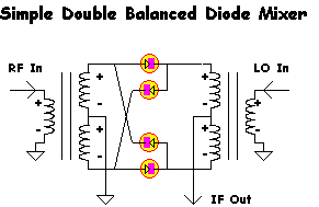
Analog IQ / RF signal processing components have been available for decades. The original offerings were constructed from two matched passive diode based "Double Balanced Mixers" (DBMs) housed inside a metal case with an integral 90 degree phase shift hybrid. This hybrid was used to combine the two DBM RF output signals or to split a single LO input into two phase quadrature LO drive signals.
These components required a reasonable amount of hand assembly and this combined with low sale volume resulted in fairly high expense per component ($US 50 to $US 150 was not uncommon). Also the tolerances introduced from complex human assembly resulted in relatively poor IQ performance.
The primary IQ/RF considerations for Analog IQ modulators and demodulators include,
| LO port to RF port carrier leakage - closely related to I and Q DC offset error | |
| RF/I and RF/Q conversion gain imbalance - caused by slight mismatching between each DBM or combining errors | |
| Inexact quadrature phase relationship between each DBM |
These (linear) IQ errors impose an ultimate Signal to Noise Ratio (SNR) limitation on modulation and demodulation performance. LO to RF carrier leakage ratios of -40 dB were not uncommon. In addition I-Q amplitude imbalance could be as high as ±0.3 dB and phase skew errors could rise to ±3 degrees. Either of these IQ imperfections could create a SNR floor limit of 30 dB. This "in band" SNR floor prohibited spectrally efficient modulation formats such as Quadrature Amplitude Modulation (QAM) which required a high SNR to achieve low Bit Error Rate (BER) performance. Passive IQ modulators where typically constrained to low order modulation formats such as BSK, QPSK or DQPSK.
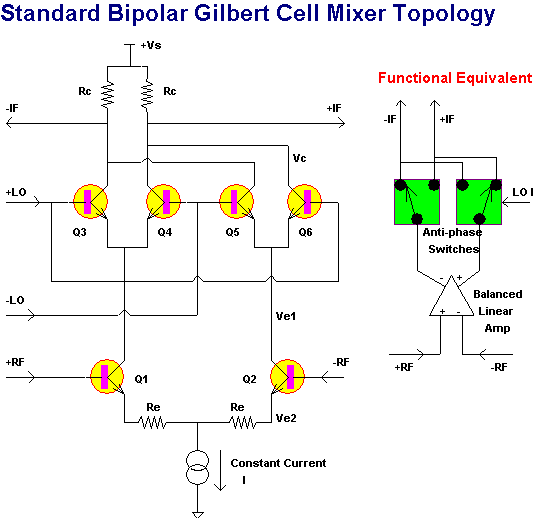
The Integrated Circuit (IC) revolution began to challenge the passive DBM's status as a RF/IQ signal processing element within the last decade or so. The "diode ring mixer" was replaced with a "Gilbert Cell" transistor mixer based on Bipolar or FET technologies. The 90 degree hybrid became implemented as a RC based network more suitable for the relative high input impedance of a Gilbert Cell LO port. In some cases the phase quadrature LO was generated digitally, using a double frequency LO divided down by 2:1 frequency dividers with inputs placed 180 degrees apart in phase (results in fLO / 2 at 90 degrees offset)
These new IC implementations offered better IQ performance resulting from the inherent matching accuracy of IC fabrication processes. In addition the costs plummeted and high performance IQ/RF Analog Modulators are now available around $US 5.00 in quantities as low as 1,000 units.
IC based Analogue IQ Modulator and Demodulator IC's now outperform the older passive DBM based versions in virtually all aspects of performance. As expectations grew from this new IC fabrication, other performance attributes such as modulation linearity and RF broad band noise attracted a focus for improvement. Modern Analogue IQ Demodulators have intermodulation performance comparable to level +17 dBm passive diode ring DBM's and corresponding Analog Modulators can an have RF output compression point limits that exceeds +5 dBm.
Even so, the Analogue Modulator and Demodulator IC's still have inherent SNR limitations - although superior to their passive diode cousins. The IQ error mechanisms may have reached a fundamental barrier based on IC fabrication tolerance limitations. This limitation is not the final word however. Analog IQ errors can be estimated and removed with a number of digitally based error correction algorithms.
I present the following articles in order to show the potential that can be unleashed when Analog IQ/RF signal processing components are combined with intelligent compensation implemented as algorithms in the digital domain. As an example, a transmitter based on an Analog IQ modulator may have an in band SNR floor limitation of -40 dB due to the three primary IQ errors (DC offset, gain imbalance, phase skew). Relatively simple ancillary hardware and appropriate digital algorithms can easily extend this SNR floor to below -65 dB. This allows QAM256 and higher to be easily converted from IQ to RF with minimal impairment.
Articles on IQ error estimation and correction for Receiver and Transmitter systems based on Analog IQ/RF signal processing are presented below.
Analog IQ to RF Architectures are especially suitable for transmitter applications. In contrast to the receiver situation, transmit signal amplitudes tend to be limited to a relatively small amplitude range, e.g. 10 ~ 20 dB - this allows a degree or relaxation on some design issues. The receiver, in contrast may be required to process signals ranging from a few uV to hundreds of mV - i.e. a dynamic range as high as 100 dB or so may be called for.
Still, the Analog Direct Conversion architecture is alluringly simple. It can be used without IQ error correction in many cases, but the cost and complexity overhead associated with Tx IQ error estimation and correction can be made relatively small with good design. I have presented one simple method that achieves this here Tx IQ Correction
I have investigate several ways to accomplish this. The first "off-line" method uses a training sequence of 8 IQ test vectors that are applied when the transmitter can be temporarily removed from service. In many applications this is not problematic as the transmit function may only be required for short, infrequent time intervals. Also, the time overhead required for training is in the region of milliseconds, and may only need to be activated over a period of hours, days, weeks or even months!
I and Q channel signals are produced from I and Q Digital to Analog Converter IC's (DAC's) usually available in a dual package. Simple IQ Low pass filtering is used to remove unwanted DAC alias output energy. These spurious outputs can be placed far above the wanted I and Q transmit spectra and may only require the addition of a simple parallel capacitor in some cases.
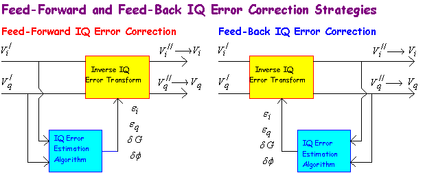
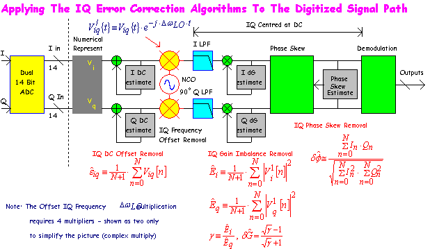
The required IQ error correction parameters (IQ DC offset, IQ gain imbalance and phase skew) can be applied to "pre distort" the IQ Baseband signal prior to the Analog IQ to RF converter. This effectively cancels out the Analog IQ errors to an arbitrary level of accuracy. The correction can either be based on a feed forward (not my preference) or a more robust "feed-back" architecture. In all cases, IQ errors are inferred from relatively easy to measure perturbations in the final RF output signal envelope (a diode detector is adequate for this)
Once estimated, the IQ error correction parameters are applied to the digital I and Q signals in the opposite order and direction to the errors generated internally in the Analog IQ to RF modulator component.
Some simplifications in the mathematics are quite feasible see my article contained here Tx IQ Correction
Some applications may not allow "off-line" correction however. For example, a terrestrial data link may need to operate in continuous transmit mode without any allowable down time (one key performance metric associated with its Quality of Service). This does not rule Direct Conversion out however (for example, data can be sent at a slightly faster rate and buffered at the receive end to leave time gaps where error estimation and correction algorithms can operate . I am currently preparing and article on methods for IQ error estimation and correction that are ideally suited to such applications (may take a few weeks to dig up my old notes on this!).
Note: Direct Conversion can represent an elegant architecture with excellent performance potential. Some implementation care is required however. Two such areas to place some engineering emphasis on include,
| Non Linear Harmonic Intermodulation In The Post IQ to RF Modulator Amplifier - The 2nd and 3rd harmonic components can mix to create a new on frequency component, appearing as additional in band noise. For example, let's image the IQ to RF modulator produces a single offset tone at (say) FRF = FLO + 1 MHz. The output at 2 · FRF with be 2 · FLO ± 1 MHz (DSB). The output at 3 · FRF will be 3 · FLO - 1 MHz. The 3rd order intermodulation terms falling at FRF will now be FRF = FLO and FRF = FLO - 2 MHz - i.e. additional noise and carrier leakage that may both degrade the overall transmitted SNR. The solution is to place a simple Low Pass Filter after the IQ to RF Modulator. | |
| RF "Re-circulation" From The RFPA to the LO VCO - The VCO will be sensitive to signals feedback at or near its oscillation frequency. This will cause frequency modulation (FM) perturbations on its output. The resulting output modulation would then be corrupted, again degrading transmit SNR. The solution is two-fold; reasonable care with layout, shielding and other isolation methods should be taken. In addition, operating the VCO at a higher frequency and dividing down by 2:1 or 4:1 will result in significant improvement. |
These two SNR degradation mechanisms may not apply to conventional approaches but can be managed with relatively little effort.
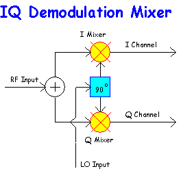
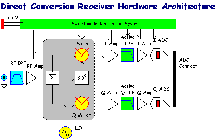
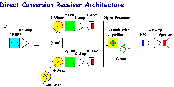
Direct conversion receivers based on the use of an Analog RF to IQ conversion component directly translate the high frequency RF signals to much lower frequency I and Q signal channels.
Amplification and Overall "roofing" selectivity is applied at IQ Baseband with relatively low complexity, low cost Op-amp or Passive LC low pass filters. The signals are then digitized with an I channel and Q channel ADC (usually a dual component) for subsequent digital signal processing. This DSP step provides the final (digitally accurate) frequency filtering, channel equalization, IQ error correction, demodulation, clock timing recovery and any other important signal processing functions.
This Direct Conversion RF to IQ architecture is equally suitable for data and analog voice communications. The appropriate demodulation algorithms are simply implemented as software code - AM, DSB, SSB or FM modulation formats are easily accommodated.
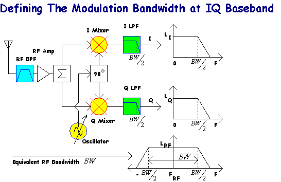
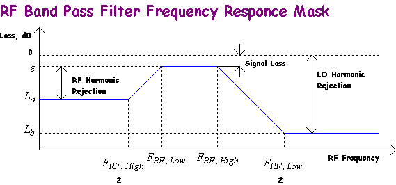
Some RF frequency filtering is required to remove (relatively minor) spurious responses. A typical fixed pre-converter mask is shown below,
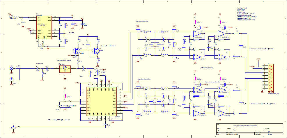
To illustrate the relative circuit simplicity offered from a Direct Conversion receiver architecture, here is an example microwave receiver RF to IQ "front End" I designed some time ago. This was intended to interface with a relatively low cost dual ADC from Linear Technology. A simple LC "anti alias" IQ low pass filter is included to prevent spurious responses caused by alias responses in the I and Q ADCs. The detailed spectral shaping filters, as required by QAM (or DFT used for OFDM) is applied subsequently in the digital processing components (e.g. FPGA).
So far we have considered a "zero IF" approach where the IQ spectrum is centrally located at 0 Hz. In some cases it may be desirable to offset this spectrum to help overcome IQ DC offset errors (i.e. the wanted IQ spectral information is shifted away from f=0 Hz so the DC offset can be removed with simple high pass filtering). I don't favor this approach though, as it introduces an unwanted image response - one of the imperfections the Direct Conversion receiver sought to overcome!
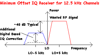
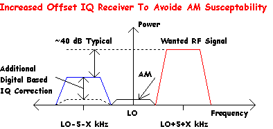
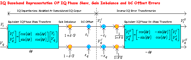
The use of IQ error estimation and correction algorithms can provide useful assistance here. Ultimate image rejection depends on the accuracy of IQ amplitude gain imbalance and the removal of IQ phase skew errors. Uncorrected image rejection may be as low as 40 dB. This could be improved a further 20 to 30 dB using IQ error correction algorithms I explain here: Rx IQ Correction
A "sneak preview" of this correction approach is shown below.
These web pages show a number of applications relevant to the use of Analog RF/IQ signal processing components in radio communication systems. Analog RF/IQ processing components do have some error mechanisms that could set a limit to overall system performance (e.g. a SNR "floor"). These error mechanisms can be largely circumvented with some intelligent signal processing operations implemented in the digital domain. Given appropriate algorithm design, exceptional modulation and RF performance is attainable with these Analog RF/IQ signal processing components, based on a low cost and complexity "Direct Conversion" approach.
I have drawn up some articles explaining some of these approaches in these following chapters,
I hope you will appreciate the potential advantages of Direct Conversion and not dismiss this technology as belonging in the "too hard" basket. It does have great potential, and missing such opportunities from previous misconceptions could be a great shame.
![]()
Return to: Ian Scotts Technology Pages
© Ian R Scott 2007 - 2008