![]()
Direct conversion (IQ to RF) architectures based on Analogue IQ Modulators offer a low cost, relatively simple approach to radio communication transmitters. The required modulation information is first converted to equivalent "In phase" It and "Quadrature phase" Qt signals containing all the required signal information. The spectrum of this IQ signal is usually centered at DC and is interpreted as having positive (+ = upper sideband) and negative (- = lower sideband) spectral components.
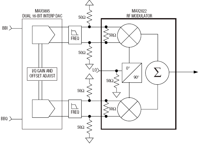
Compared to Direct RF Signal Synthesis (DRFSS) or IF to RF conversion based on a Superhet transmitter architecture, Direct Conversion offers a considerable reduction in hardware cost and complexity. The Digital To Analogue (ADC) converters used to generate I and Q signals only need to sample at twice the upper I or Q spectral component energy to correctly digitize the wanted transmit information prior to IQ to RF conversion. Even if "over-sampling" is used to alleviate the performance requirements of post ADC anti-alias rejection filters, the actual sample rate is much lower than the requirements of DAC to IF generation (superhet approach) or direct DAC to RF generation (DRFSS).
For example, consider a microwave QAM transmitter with a transmit spectral bandwidth requirement of ±1.5 MHz and a final output frequency of 2.65 GHz. A Direct Conversion IQ to RF conversion architecture will require each I and Q DAC to have a sample update rate of at least 3.0 MHz, and 10 MHz sampling rate would be reasonable. This I and Q "Complex Baseband" information would then be converted directly to the required RF frequency of 2.65 GHz using an Analogue IQ Modulator (IC or DBM) with a single LO input frequency also at 2.65 GHz.
In contrast, an IF to RF superhet approach would probably require two frequency conversions. For example,
DAC_IF Output @ 10 MHz IF_1 -> IF_2 @ 325 MHz -> RF Output at 2.65 GHz
The minimum DAC sample rate would be 20 MHz, but it would be preferable to over-sample at (say) 65 MHz or higher. High speed, high resolution DAC's increase sharply in price compared to their lower sampling rate cousins. Even if the difference is slight, the additional cost and complexity of a dual conversion superhet transmitter is unattractive. (requires two LO frequency synthesizers, two up conversion mixers and associated image and LO leakage reject filtering).
The DRFSS approach is probably infeasible at such frequencies based on today's DAC technology (and the speed of FPGA interface logic). A DAC would need to sample at least at 5.5 GHz to reconstruct this RF signal output (although an alias output could be used, as in sub-sampling, sample and hold based DAC's have a sinc{x} frequency roll-off characteristic and impaired linearity when used in a sub-sampling mode).
The Direct Conversion IQ to RF architecture certainly appears welcome in comparison! However this method has some (potential) limitations,
| Finite IQ linearity resulting in potential "spectral re-growth" - extending actual occupied RF bandwidth. | |
| Transmit Broad Band Noise - elevates overall background noise floor over a wide frequency range | |
| Residual LO to RF Carrier Leakage - causes a Signal to Noise Ratio (SNR) impairment. | |
| Spectral "Spillover" between upper + and lower - sideband components of the transmitted signal. |
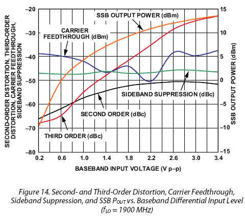
The first linearity impairment is usually solved by operating the IQ Modulator at a reduced IQ drive level. Usually 5dB to 10 dB "drive back-off" will be adequate. Some IQ modulators (e.g. Analog Devices AD ) have internal IQ linearisation built in to reduce the need for IQ drive reduction. Improvements in device technology is on going. The issue of broad band noise is also being addressed. Early IQ modulators had broad band noise floors as high as -130 dB1Hz! Modern IQ modulators can offer broad band noise floors better than -170 dB1Hz.
(Note - some IQ modulators are specified with noise output in the absence of IQ drive. This can be misleading as broad band noise can increase by 10dB or more when modulation is applied to an Analogue IQ Modulator IC)
The last two imperfections show some improvement with technology advances but are likely to remain as potential weaknesses and contribute to a degradation in Signal To Noise Ratio (SNR) associated with the transmitted modulation. These IQ errors can present a SNR "floor" as low as 30 dB. To illustrate the importance of this, I have run a simple MATHCAD simulation for various levels of Quadrature Amplitude Modulation (QAM) based on some (admittedly) approximate mathematics!
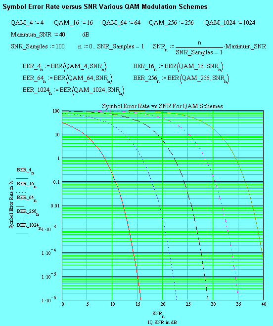
Note: I have used actual RF SNR as the "x" variable as opposed to "Energy per bit" definitions. The actual RF bandwidth is centered around the RF carrier (at fLO) and has twice the occupied bandwidth of I and Q channel spectral energy (BWRF = 2 * BWI = 2 * BWQ ).
The good news is that the Analog IQ errors can be corrected completely at IQ Baseband (in the digital domain). My article (following) shows exactly how this can be accomplished.
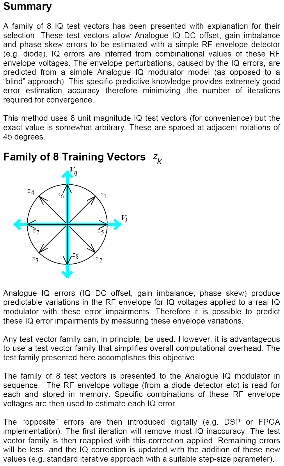
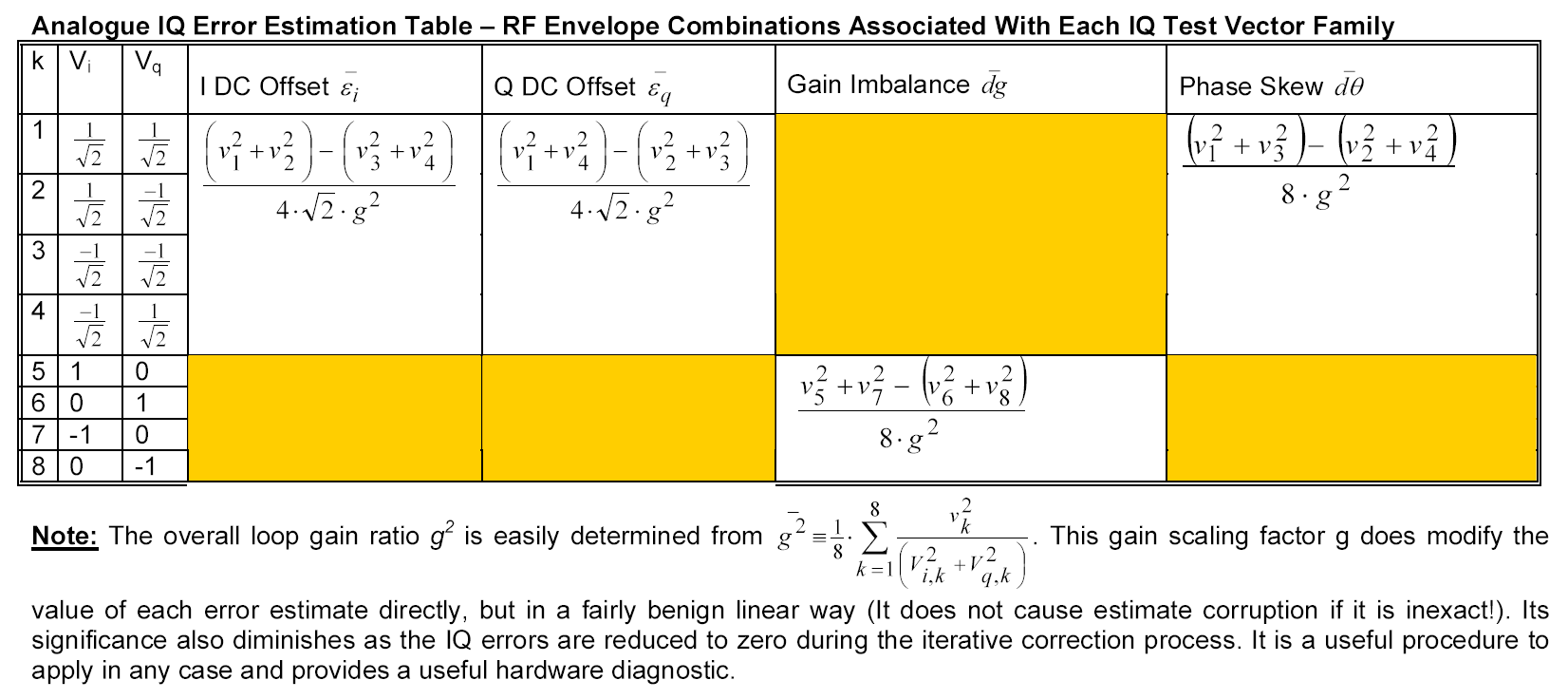
A simple method is described, based on a family of 8 IQ DC test vectors and monitoring the resulting RF envelope signal (e.g. with a simple diode detector). Variations in the envelope voltages are used to infer each IQ error. The inverse error correction mechanism is then applied in the digital domain thereby canceling the overall IQ errors out.
The errors targeted by this "off line" method are
| I DC Offset Imbalance - causes carrier leakage | |
| Q DC Offset Imbalance - also causes carrier leakage | |
| Relative IQ Gain Imbalance - causes spectral "spillover" between upper + and lower - sideband components of the transmitted signal. | |
| Relative LO Phase Skew Imbalance - also causes spectral "spillover" between upper + and lower - sideband components of the transmitted signal. |
The method is applied iteratively until all errors are cancelled to an adequate level. This procedure is applied "off-air" and infrequently (IQ errors tend to be very stable over time). After satisfactory convergence is obtained, the IQ corrected transmitter is allowed to transmit actual RF signals with exceptional modulation accuracy.
Note: I have also developed an "on-line" error correction strategy that I will describe soon.
All Analogue IQ Modulators exhibit some carrier leakage from their Local Oscillator (LO) input to their RF output port. This has the effect of degrading in band Signal To Noise Ratio (SNR) performance on transmit. For example, residual LO carrier leakage at -40 dB from the wanted modulated output is equivalent to an in band SNR of 40 dB. The Bit Error Rate (BER) performance of high level QAM (e.g. QAM32 and higher) may be adversely affected by SNR noise floors around these levels.
LO carrier leakage arises from two main mechanisms,
| Direct carrier leakage due to parasitic coupling between elements inside and surrounding the IQ Modulator. | |
| Inexact gain and phase matching between mixing elements contained in the internal Double Balanced Mixers (DBM) - An Analogue IQ modulator contains two such mixers driven with a quadrature phase LO. | |
| Inexact DC offset cancellation at the IF port of each internal DBM. |
Although the mechanisms may be different, all are functionally equivalent to the presence of DC offset errors at the I and Q input ports of the Analogue IQ modulator. It follows then, that if an equal and opposite I and Q DC offset voltage is applied to these ports, the resulting LO to RF leakage will be cancelled to zero.
This next diagram and associated mathematics
shows a model for LO to RF leakage "referred to IQ Baseband"
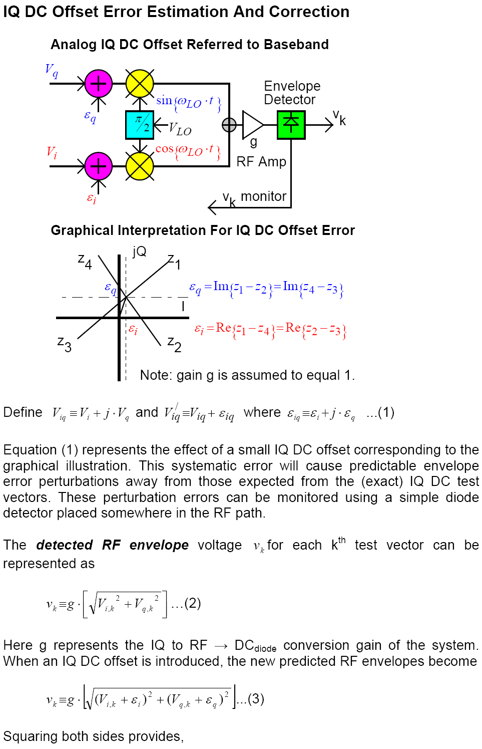

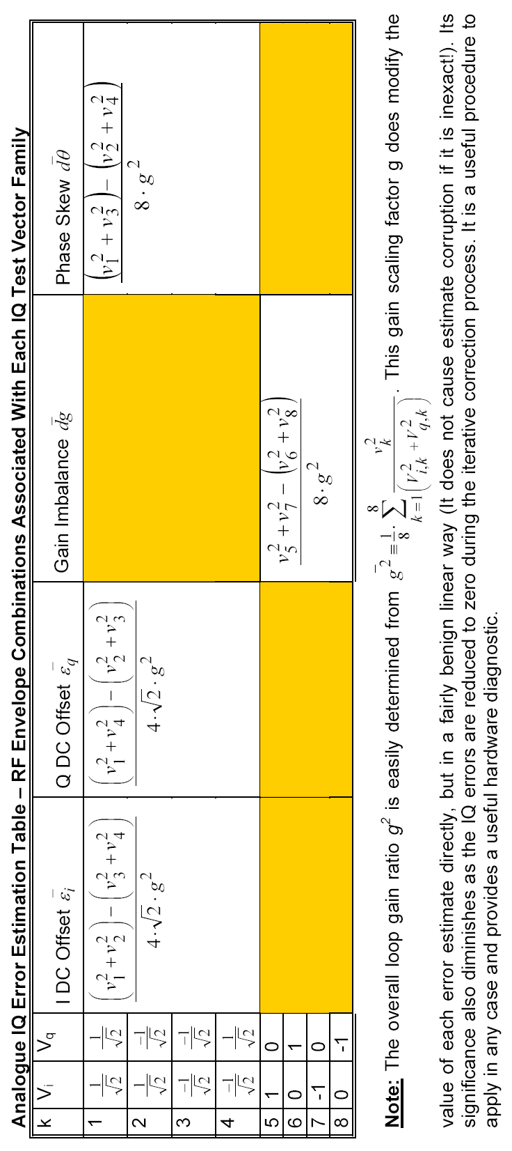
Equation (8) shows how each I and Q DC offset can be derived from the measured RF envelope voltage combined with each kth IQ test vector and a knowledge of the overall system gain "g" (which can always be scaled to a convenient value of one either in hardware or as a digital scale factor multiplication).
I and Q DC error estimates depend on each other, but suitable selection of I and Q test vectors can eliminate this dependency. The I DC offset error estimate requires two test vectors k and k' to have equal Q values and the Q DC offset error estimate requires The k and k' I values to be equal,
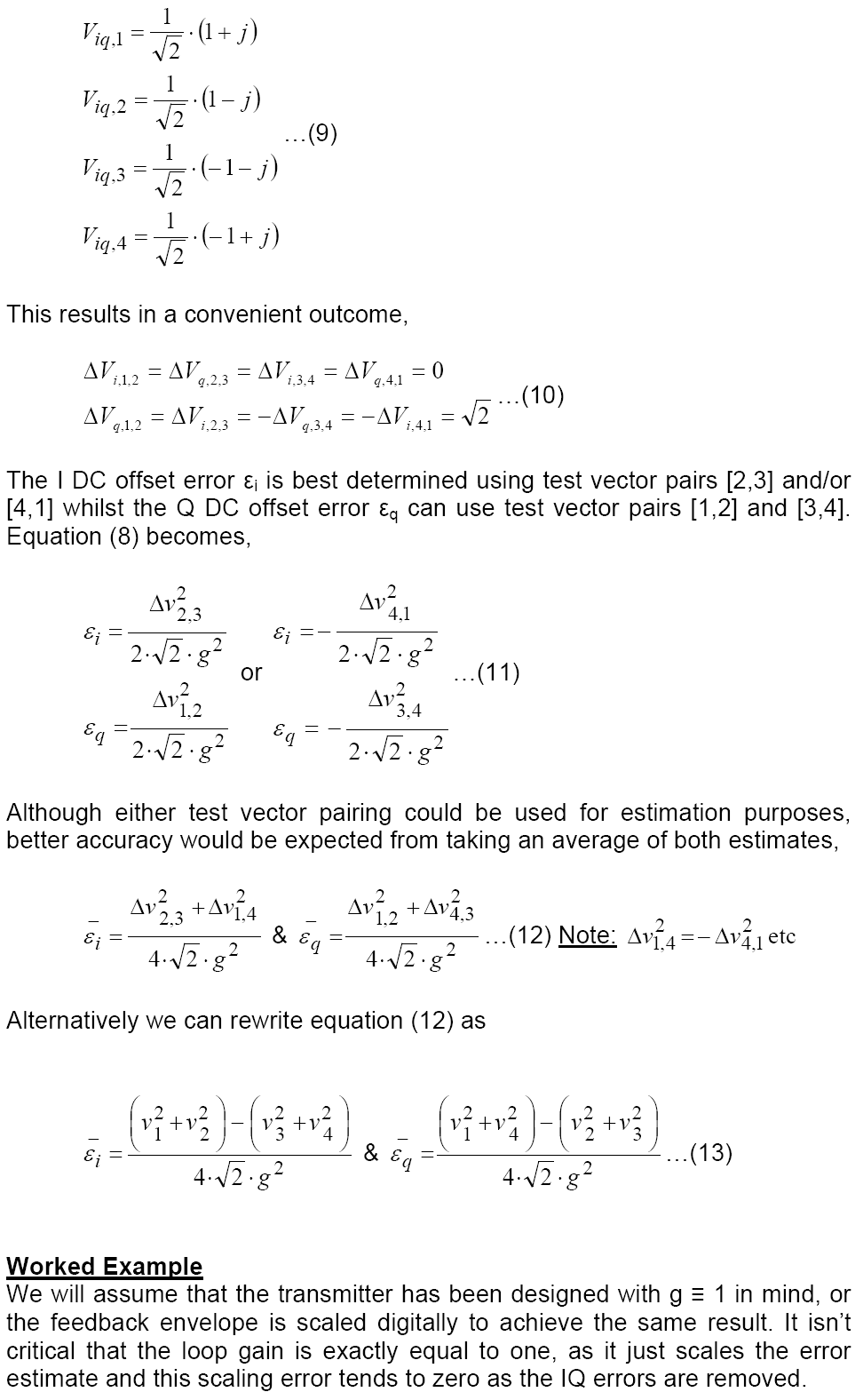
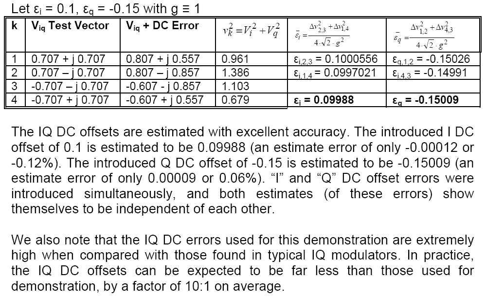
The four IQ test vectors selected allow two estimates for I DC offset and two for Q DC offset. Averaging both dual estimates improves accuracy and results in a simple computation shown in equation (13). A worked example follows, using extremely high DC offset errors in order to demonstrate the method's robustness to error.
All Analogue IQ Modulators exhibit some cross coupling between upper and lower sideband energy at their RF output port. This is usually measured for a single IQ carrier input based on a cosine (I channel) and sine (Q channel) signal source.
Under these conditions, and "ideal" Analogue IQ modulator would produce a single RF output carrier with a frequency equal to the LO input frequency + the IQ sinusoidal tone frequency. If the Q channel polarity is inverted, the RF output carrier would equal the LO carrier frequency - the IQ sinusoidal modulating frequency.
Real Analog IQ modulators are not perfect (of course) and some residual "other sideband" RF carrier leakage will be observed. As in the case of LO carrier leakage this represents another in band SNR degradation mechanism. For example, a sideband suppression ratio of -40 dB from the wanted modulated output is equivalent to an in band SNR of 40 dB. When actual modulation is applied, spectral energy from upper and lower sideband regions will intermingle causing in band interference. The Bit Error Rate (BER) performance of high level QAM (e.g. QAM32 and higher) may then be adversely affected by this degraded SNR floor.
Two primary mechanisms are responsible for the intermingling between upper and lower spectral energy components,
| The Analog IQ Modulator has internal DBMs with slightly different conversion gains. This gain imbalance prevents exact cancellation of the unwanted sideband component. | |
| The Analog IQ Modulator an inexact phase quadrature LO source for each of its two internal DBMs. This "phase skew error" also prevents exact cancellation of the unwanted sideband component. |
If one of the internal DBMs has a slightly different conversion gain, it is perfectly reasonable to expect that its I (or Q) drive is simply scaled up or down in level to compensate. This analysis assumes that one DBM will have high conversion gain, and the other will have lower conversion gain. This symmetry is mathematically convenient as it tends to preserve an average conversion gain.
We will normalize average conversion gain "g" to unity for convenience, as this scaling can always be accomplished without effort. The individual I and Q conversion path gains will be represented as g = 1 ±dg.
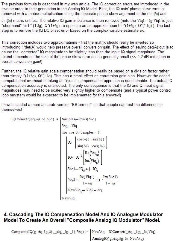
Note: To be pedantically exact, the "I" correction gains should be be gI' = gI / (1+dg) and the "Q" correction gain should be gQ' = gq /(1-dg) but dg is assumed to be small so the binomial approximations 1/(1+dg) ~ 1-dg and 1/(1-dg) ~ 1+dg seem reasonable. Given that "division" is more computationally intensive than addition and subtraction this "purity" seems unjustifiable considering the minimal estimation error introduced. The importance of any such inaccuracy further diminishes as the gain imbalance error is removed (a relative gain imbalance only requires a single variable). The minor consequence of this approximation is to introduce a small global gain scale error. Since RF amplifiers have frequency and temperature dependent gain anyway, this global gain modification would be corrected by existing output power management and control systems anyway.
The next analysis shows the method for determining this gain imbalance, followed by another analysis showing how to derive phase skew errors in section 2.3.
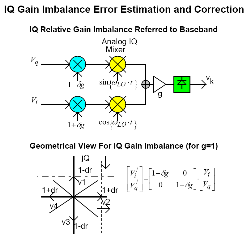
Relative IQ gain imbalance uses a different set of IQ test vectors compared to the previous case of IQ DC offset error.
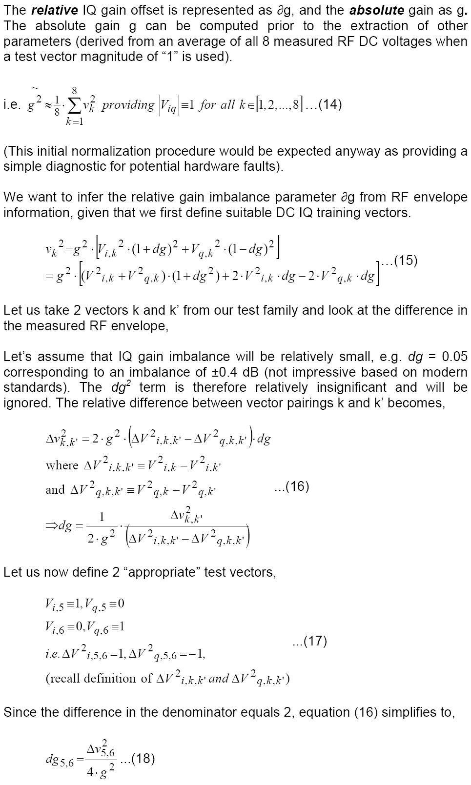
Equation (18) shows how one IQ test vector pairing (k=5,6) can produce a gain imbalance estimate dg. However this estimate can also be obtained from 3 other possible pairings. Each estimate may suffer from various accuracy limitations, so it makes good engineering sense to assemble and average of all four, given that each estimate is no better or worse, on average, than the other.
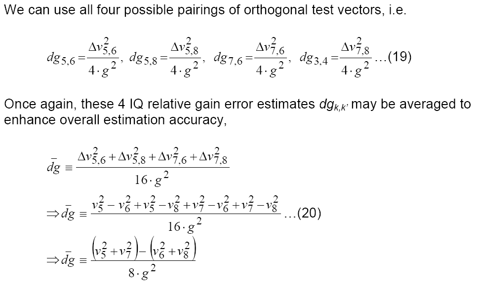
All four RF envelope values vk are used corresponding to IQ DC test vectors where k = [5,6,7,8]. We will demonstrate the method's error estimate extraction accuracy with an example (excessively high) IQ gain imbalance of dg = 0.05. This corresponds to a gain imbalance of +0.42 dB or -0.45 dB.
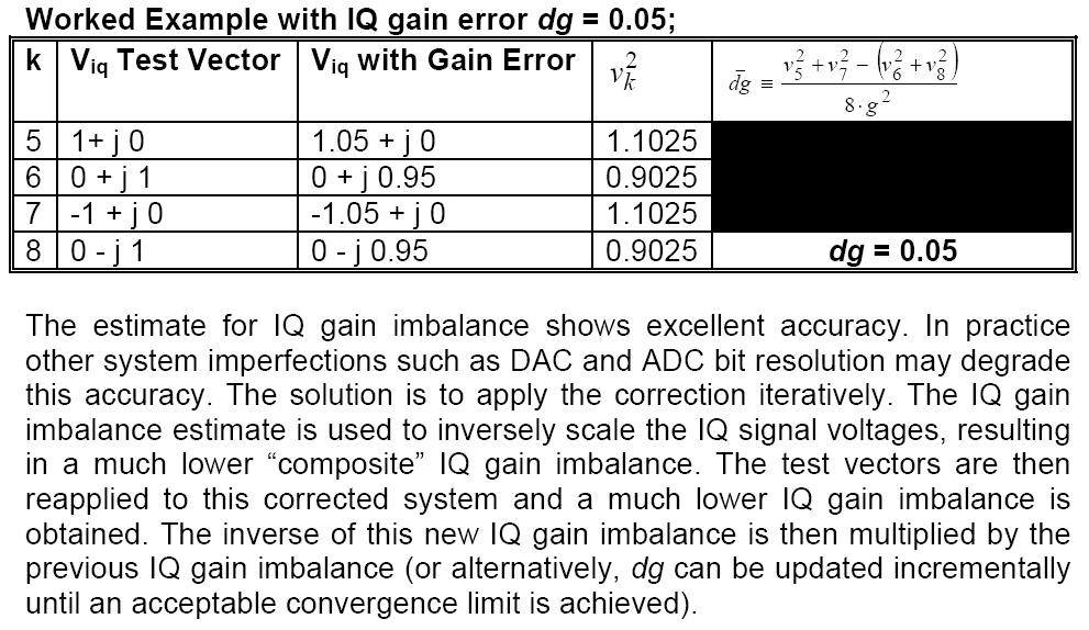
Note: A reasonably "good" Analog IQ modulator will have an IQ gain imbalance less ±0.1 dB, corresponding to a sideband suppression ration or -40 dB. The extremely poor IQ mixer used for this demonstration shows the estimation method to be extremely robust.
As mentioned previously, inexact quadrature LO phase phase also degrades in band SNR from cross coupled energy between upper and lower RF sideband spectral energy. It is not unreasonable to expect that an equivalent effect would be obtained by cross coupling I and Q signal energy presented to an "ideal" Analogue IQ Modulator without phase skew errors. We will represent this mechanism as a phase skew matrix operation that rotates I and Q axis' in opposite directions (i.e. not a rotation in which both axis rotate the same way!)

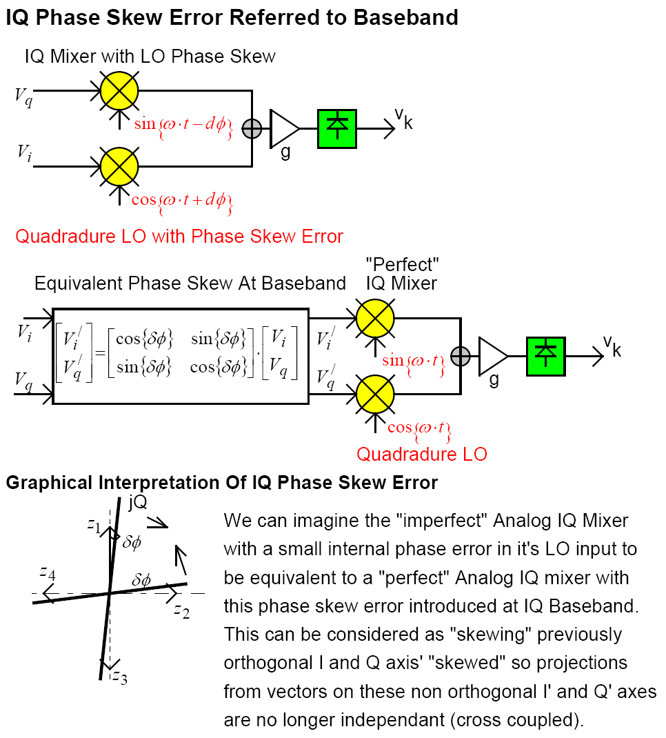
If FM or FSK is presented to such a mixer suffering from phase skew error, the output constellation will appear as an ellipse instead of a circle.

The phase skew error is estimated from one pairing of IQ test vectors. However three other pairings are possible (in which the denominator is not equal to zero!).

Once again the use of an average of all four estimates represents good engineering practice and leads to best expected phase skew error estimation accuracy. An example is now shown with a relatively high phase skew error of 3 degrees (1 degree is more typical in real IQ Modulators).
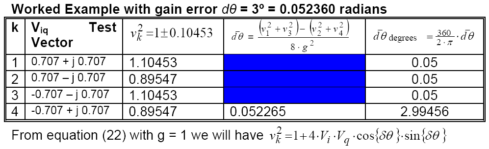
Note: The phase skew error estimate is derived with excellent accuracy. It is standard practice to work with angular units in radians, but degrees are often more "comfortable" to conceptualize.
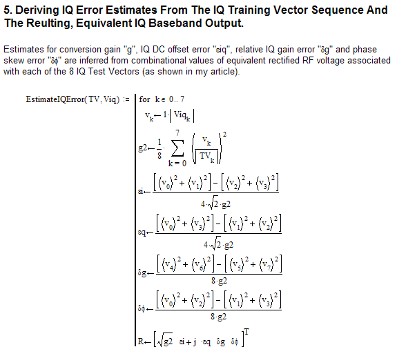
The 4 IQ error parameters are derived from this "Model Based Parameter Estimation" approach based on the use of 8 IQ test vectors and measurement of their corresponding RF output voltage magnitudes using a simple detector. The test vectors k=[1,2,3,4,5,6,7,8] can be applied in any order that is convenient and the corresponding RF envelope voltages stored as v1, v2 ,..., v8 .
I hope this article helps people to achieve the optimum possible performance from Direct Conversion Transmitters based on Analog IQ Modulation. The hardware overhead for this IQ error estimation and correction method is minimal, comprising of a simple diode detector (high linearity is not essential and dynamic range requirements are extremely relaxed - the RF level input is always at a near constant level during training.)
The actual training ritual is best applied iteratively, even though the first iteration may provide near exact IQ error correction. The updated IQ error estimates, following each iteration, will show diminishing magnitude, tending to zero as convergence is achieved.
Without this correction, typical Analogue IQ modulators will exhibit LO carrier and sideband leakage between -35 and -40 dB. The correction obtained with the procedure described is usually better than -65 dB. This is clearly a massive improvement, and one that remains stable with time.
(I intend to describe a second method soon that avoids the need for off line test vectors. A simple diode envelope detector is still used but wider bandwidth and linearity requirements are assumed.)
Note: Even communication systems that require near 100% availability can still use "off line training" by sending Tx data in packets at a slightly faster rate than required to allow a time gap for training. A data buffer in the remote receiver would then simply supply continuous output data at the correct, slightly lower data rate. The only downside I see to this is the introduction of some data latency (i.e. delay in data throughput) but the acceptance limits on this depends on the actual application's latency requirement (no system can ever have zero latency as radio waves still have to travel at 3 · 108 m/s! - e.g. a separation of 50 km implies a path delay of 1.67 milliseconds anyway!).
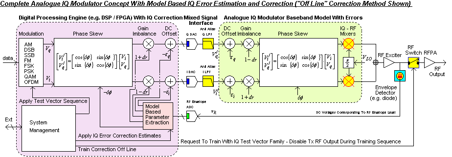
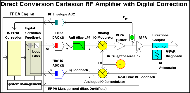
These following diagrams show the overall architecture for a practical Direct Conversion Transmitter based on Analogue IQ Modulation combined with IQ error estimation and correction. This correction is applied "off line" during times when actual transmission of data is not required.
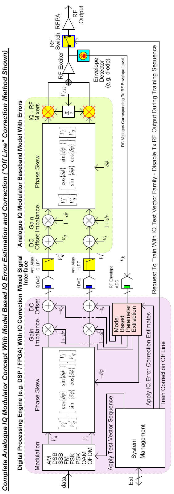
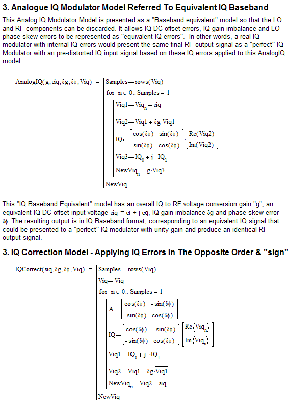
This MATHCAD file uses the previous 8 IQ Test Vectors with a slight modification where k = 0,1,...,7 instead of k = 1,2,...,8 as this suits matrix and array operations. The "AnalogIQ" function introduces IQ DC offset, IQ gain imbalance and IQ phase skew errors as equivalent complex Baseband error terms and produces a new distorted version of Viq corresponding to the introduction of these errors.
This AnalogIQ function is then called up in the "EstimateIQError" function. This compares the equivalent RF envelope voltage (that would be produced by a real imperfect Analog IQ modulator with these errors) against each IQ Test Vector as per the estimation procedure shown previously. These inferred IQ error estimates are transferred to the array "R".
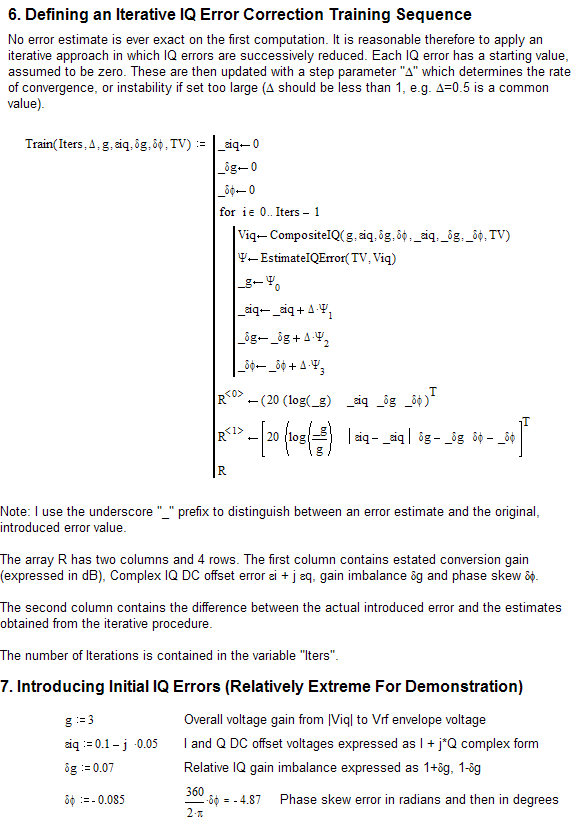
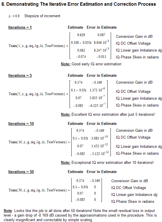
Some arbitrary IQ errors are introduced and the "EstimateIQError" algorithm was used to infer them. The first iterations were quite successful. Further iterations showed significant improvement. The IQ errors were rapidly estimated with extremely good accuracy.
Consequently the use of an "off line" IQ error estimation and correction procedure does not appear to be problematic. Its key features are,
| Its hardware implementation has low cost and complexity | |
| The need for periodic "retraining" is unlikely as these errors tend to remain quite stable over time, and show slight variation over temperature extremes. | |
| The number of iterations required for convergence is small - perhaps 5 or less. If each iteration takes as long as 1 millisecond, the transmitter only needs to be "offline" for 5 milliseconds to perform the IQ error correction ritual. |
If the transmitter cannot afford to be "offline" for any period, e.g. as may be a constraint required of a critical microwave data link, then Analog IQ modulation can still be used but a slight modification to the approach is called for. I hope to publish this method soon (on this web site!). However it may well be easier to just use the use of a receiver buffer and send data slightly faster than required to leave a training gap as suggested earlier.
This more generic method uses the IQ values "as is" to represent test vectors, and the envelope variations are compared with these IQ values to infer IQ errors in real time, on line.
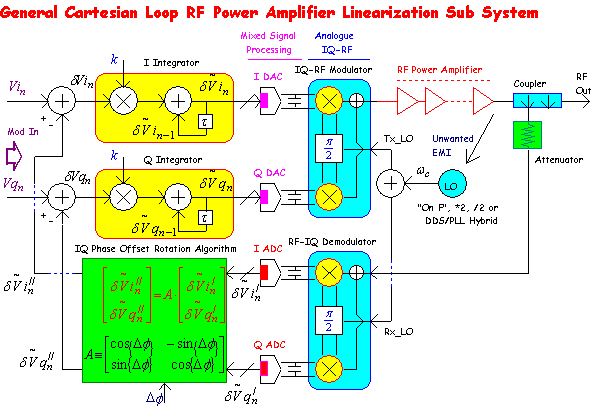
Analog IQ modulation is often associated with RF PA linearisation based on a "Cartesian Feedback" approach. This architecture is most suited for narrow bandwidth modulation formats such as TETRA DQPSK or TR8.12 "Tetrapol" FSK.
Negative Feedback is applied at IQ Baseband, as opposed to the actual RF frequency. The comparison between forward (Tx) and reverse (Rx) IQ paths can be performed with analog components, or in the digital domain (as shown). The digital approach allows any phase offset correction to be applied digitally - avoiding the need for an extra Analog LO phase rotation component.
A Cartesian linearisation architecture based on Analog IQ/RF Up and Down conversion, combined with digitally implemented phase rotation and negative feedback with a simple loop filter (for stability) can be represented as follows,
This architecture is very suitable for narrow band technologies such as those used in PMR (Public Mobile Radio) applications. This includes TETRA DQPSK Modulation and "Tetrapol" TR8.12 Modulation Formats. These modulation formats typically have spectral bandwidth requirements of about 20 kHz. The mixed signal devices (ADC and DAC) still require medium to high sample rates (e.g. 40 MHz or higher) in order to allow a high effective "open loop bandwidth" so that ample loop gain is available within the IQ modulation bandwidth for non linearity correction caused by RF Power Amplifier artifacts. The ADC "latency", i.e. how many clock cycles are needed to transfer an acquired signal to its digital output bus, is also important and this loop delay time limits the unity gain bandwidth.
In practice, a closed loop unity gain bandwidth 300 kHz or greater is possible, and Adjacent Channel Sideband Power (ACP) reductions of 15 to 20 dB are readily attained with medium cost components.
The concept can be enhanced (almost indefinitely) by using a "nested loop approach". This places a Cartesian Corrected RF PA loop inside an outer Cartesian Corrected RF PA loop, thereby extending the correction potential for non linear artifacts. (This approach of nested loops is common practice in audio amplifier design!). Of course the loops do not all need to be Cartesian - here is an example of a Polar Feedback system enclosed in an outer Cartesian Feedback correction loop.
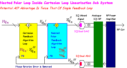
Additional "outer loops" can be added if required. The ultimate correction potential depends on the IQ Demodulator performance. Since this is placed in the feedback, any distortion introduced by the IQ demodulator will show up on the RF output. The simplest solution is to run this component at a reduced RF input level so that its linearity improves.
Then the IQ error correction procedure may become more relevant as IQ DC offset errors will become more significant compared to a reduced IQ output signal level.
Still, I hope this article shows the wide relevance that Analogue RF/IQ
device technology has to radio communication systems. The Direct Conversion
architecture is a personal favorite of mine, and can benefit greatly from
enhancement processing implemented in the digital domain (DSP or FPGA devices).
Unfortunately not all radio product manufacturers are aware of these error
estimation and correction algorithms (or perhaps any?). Perhaps this article
will help to shed some light
 on methods suitable for Direct Conversion performance enhancement.
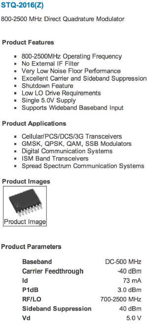
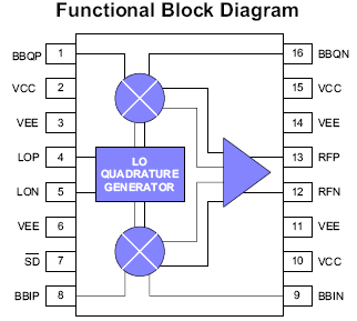
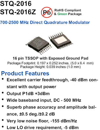
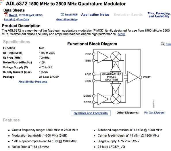
Several companies have invested significant R&D resource into the development of high performance Analog IQ Modulator IC's. Although originally spanned by passive diode based component offerings, these components have largely lost favor in the industry due to excessive cost and mediocre IQ performance. They also tend to have relatively low RF operating bandwidth. IC implementations, in contrast, are usually far superior in all aspects.

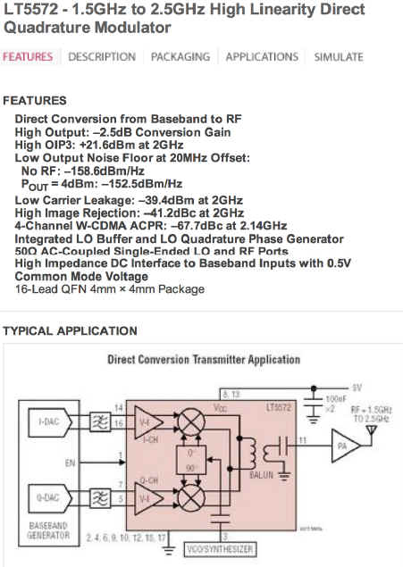
Note: The LT5518 application shows the use of a diode detector for IQ error correction - but there is no need for a dual output! It appears that Linear Technology is unaware of the much simpler IQ error estimation and correction procedure I have just described!
They do make great RF IC's though!
Note: The use of a direct DAC to IQ interface is a great bonus! This usually requires a center IQ input voltage equal to 0.5 V.
![]()
Return to: Analog IQ
or: Ian Scotts Technology Pages
© Ian R Scott 2007 - 2008