![]()
A "Software Defined Radio" or SDR consists of a transmit path and a receive path with a common digital signal processing interface. Unlike a traditional radio, a SDR uses digital signal processing to process signals as opposed to specific hardware. The SDR concept seeks to "move the analog to digital" processing as close to the antenna port as possible, leaving any associated hardware as fulfilling a "transport function" or other supporting roles such as power supply reticulation.
This article examine the receive path for a SDR. The ultimate goals of a SDR receiver include,
| Arbitrary Modulation Format Decoding Capability | |
| Software Defined Signal Bandwidth and Data Rate Acceptance | |
| Minimal RF Signal Processing - Antenna to ADC connectivity only | |
| Ability to Receive Multiple Signals | |
| Ability to Receive Multiple Signals Of Arbitrary Incompatible Formats and Data rates |
This philosophy would lead us to consider such a SDR to consist of an antenna connected to the input of an Analog To Digital Converter (ADC) followed by a fast digital computational engine. Although this may happen as technology improves, current ADC devices still have specific limitations,
| Finite Bit Resolution - Sets an upper limit to dynamic range | |
| Finite Sample Rate - Also limits dynamic range, but also maximum acquired signal bandwidth | |
| Alias Responses - All time sampled signals have multiple alias responses that require ancillary hardware based filtering | |
| Current consumption - High sample rate devices draw considerable power - this limits applications to small portable receivers | |
| High Cost - ADC devices at the forefront of mixed signal conversion technology come at a premium price. General purpose ADC devices can offer multiple converters in a package for less that $US 2, whilst a high performance 2 GHz ADC could cost more than $US 500. |
So although the ultimate SDR concept represents a desirable goal, its implementation may be too problematic for many applications, especially those that don't need all its potential features.
For some people, "SDR" may refer to a product that has its main signal parameters defined in software. Such a radio may have some hardware imposed upper limits on demodulation bandwidth, data rate or format capability but allow some flexibility within these constraints. The radio may also be incapable of receiving multiple signals within a frequency domain "cluster" or it may be potentially capable of this but only if all received signals share the same modulation format and data rate.
Receivers based on this "cut down" SDR functionality reduce development overhead and cost by "protecting" the ADC with a preceding band pass "roofing filter" This removes unwanted alias ADC responses and also reduces the probability of excessively large signals appearing at the ADC input, that could lead to saturation. Further, a super-heterodyne approach is needed to allow RF frequency agility. Such a receiver can therefore be programmed across a wide range of receiver "frequency chunks" and have the potential to digitally narrow this captured spectrum down to a more appropriate value.
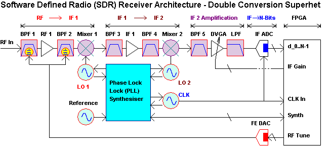
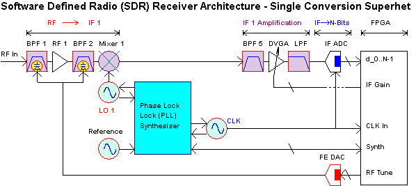
For frequencies up to 1 GHz, a double conversion super-heterodyne architecture may be most suitable for this limited SDR receiver. The first "IF 1" frequency is chosen to facilitate image and "½ IF" rejection in the first frequency down conversion sub system. A suitable first IF frequency range between 45 MHz and 90 MHz may be suitable for a "SDR" receiver intended to cover a 400-520 MHz frequency range. The image and ½ IF Band pass filters BPF 1 and BPF 2 will need to be electronically tuned in this example (varicap diode tuning can achieve input third order intercept point (IIP3) levels greater than +20 dBm if designed properly). The first LO 1 frequency will be programmable using a conventional Phase Locked Loop frequency synthesizer approach. This results in a fixed IF 1 frequency with filters BPF 3 and BPF 4 intended to set an upper bandwidth "roofing" limit for the receiver. These filters could easily be monolithic quartz crystal based or Surface Acoustic Wave (SAW) versions.
Many cost effective ADC components can process these relatively low IF frequencies without much difficulty. However, in some cases a second frequency conversion from IF 1 to IF 2 may be appropriate. In the "Multiple User Software Configurable Arbitrary Format" MUSCAF receiver described in my RAWCON98 presentation - MUSCAF Rx - I used a 10.7 MHz IF filter for BPF 5 at IF 2. This provided a "roofing bandwidth" of 200 kHz, allowing 16 adjacent channels of 12.5 kHz to be received simultaneously as a "cluster", or a single channel up to 200 kHz modulation bandwidth.
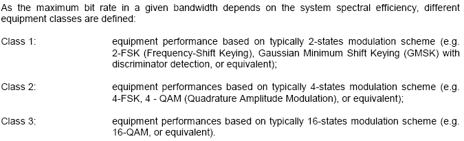
This demonstration hardware was based on suitable components at the time and provided an indication of SDR concepts and potential. The dual conversion approach would not be my first choice for frequencies below 1 GHz now of course! A dual conversion approach may be quite appropriate for a microwave data link at 2.1 to 2.7 GHz though (ETS 300 633) and a flexible single channel bandwidth, modulation format and data rate capability would be extremely advantageous as outlined in this standard for classes 1, 2 and 3.
In this application the first IF 1 could be selected as 280 MHz of 325 MHz based on available wide band SAW filters at these frequencies. The second IF could be around 70 MHz and the ADC could be used in a "sub sampling" mode - i.e. using a higher frequency alias as a "wanted" response to keep cost and current consumption low.
Each frequency conversion process adds cost, complexity, PCB real estate area and the potential for additional spurious responses. It is desirable to minimize the number of such frequency conversions (Note: Frequency conversion stages are usually best designed with zero dB conversion gain - otherwise subsequent conversion stages will experience premature overload, so little real benefit is provided by additional frequency down conversion stages).
Many high resolution, high speed ADC devices can acquire signals much higher than their sample rate with little performance deterioration. For example, a medium low cost 14 Bit ADC clocked at 40 MHz can easily capture input signals as high as 350 MHz on a high alias response (in this example, the lower 9th alias at 9 · 40 MHz = 360 MHz will result in a captured digital output frequency centered at 360 MHz - 350 MHz = 10 MHz).
Using the previous UHF example covering a frequency range of 400 - 520 MHz, the use of a first IF frequency of 70 or 90 MHz would equally produce a 10 MHz ADC digital output, based on a 40 MHz clock and the use of a 2nd lower or upper alias zone respectively.
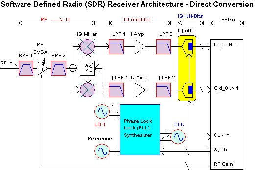
If further complexity reduction is sought, Direct Conversion based on Analog RF to IQ conversion may be the answer. This can offer quite high IQ bandwidth potential, up to ±100 MHz = 200 MHz (total) is not unreasonable. This would definitely suit an ETS 300 633 application at 2.1 to 2.6 GHz (for set-up convenience as external, manually tuned duplex filters would ultimately restrict operational frequency range). Further, any SNR degradation mechanisms caused by residual I and Q DC offset errors become less important in wide band receivers simply because wide band signals need more power than narrow band signals so DC offset errors become small by comparison.
Current Analog IQ Demodulator IC's provide exceptional, robust RF performance and IQ accuracy. For example IIP3 values exceeding +23 dBm are common combined with Noise Figures below 13 dB. IQ gain imbalance errors can be as low as 0.1 dB and phase skew errors less that 0.3 degrees. Consequently, Direct Conversion architectures are no longer a "bubble gum" cousin to a superhet.
The "ultimate" SDR receiver offers complete software configured functionality and performance. Although it could be based on a superhet or direct conversion architecture, the additional RF, IF, and or IQ signal processing stages involved can only be seen as sources of signal degradation (noise, distortion, etc), complexity and cost. From this perspective, an ambition to remove as much RF signal processing as possible is indicated. The only "allowable" RF signal processing stages include anti alias Band Pass Filters, wide dynamic range RF amplification and possibly a Digitally Controlled Variable Gain Amplifier "DVGA" (may contain a digitally controlled attenuator) included to minimize the danger of ADC overload.
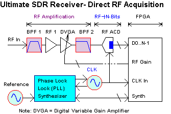
This "puritanical" philosophy may not suit all application requirements though - that is the "Software Defined Radio" may never be a "one shoe fits all" offering given other real world considerations. By relegating RF signal processing to that of "signal transport, minimal corruption" only, demands on the Analog to Digital Converter escalate. These demands become more problematic as the upper operational frequency range is extended.
ADC technology has come a long way and enjoys continuous improvement. Equally, digital processing engines such as FPGA (Field Programmable Gate Array) devices have largely kept pace. For example, a single FPGA may contain 2,000,000 programmable logic elements capable of operating at clock rates up to 2 GHz. These elements can be configured in software to form FIR and IIR digital filters, multipliers, numerically controlled oscillators, decimation and interpolation chains, equalizers as well as demodulation and clock recovery algorithms. Further, the FPGA logic elements can operate completely in parallel - this is a major advance over previous DSP devices that remain largely sequential in operation with some parallel processing capability.
This computational engine is well suited to the ultimate SDR and smaller versions are very cost effective (e.g. less than $US 10 in reasonable quantities). They are, by their nature, extremely generic and can be made to emulate microprocessor functions or PC CPU functions as well.
A significant advantage of FPGA processing involves the protection of Intellectual Property (IP). Hardware designs can be copied relatively easy - removing IC markings does not prevent an electron microscope can on the internal die for example. Any product based on a hardware intensive approach is therefore subject to the risk of IP theft.
However it must be asked - who really needs an ultimate SDR Receiver or "DRFSA" ? Some possible end user groups include
| Spectrum Surveillance Services - Fast Monitoring Illegal or Disruptive Signal Sources (especially if intermittent). | |
| Search For Extraterrestrial Intelligence "SETI" - Searching for "a needle in a haystack" signal amongst a wide channel of background noise. | |
| Ad-hoc Emergency Radio Services Deployment - To re-establish lost communication services during civil emergencies involving loss of radio infrastructure connecting ambulance, fire and police, each having unique modulation formats, data rates, user group codes etc. | |
| Radio Amateur Groups - A DRFSA for HF (i.e. frequencies below 30 MHz) could be fairly inexpensive and considered as a hobby item. | |
| Military Applications - Co-ordination of multiple services with independent encryption and modulation format categories. |
In many cases, just having an appropriate degree of software programmability may be more than adequate, and a "compromise" SDR architecture may be preferred. There is of course nothing wrong with this approach as technology should always be matched to the customer's required application.
The next chapter will now examine some of the technical challenges associated with an "ultimate SDR" receiver. This will be based on available device technology, with some speculation as to possible improvements that may be expected over the next 5 years or so.
The predictive overall performance specification for a DRFSA SDR is largely determined from the RF performance associated with its selected RF ADC. A short ADC comparison summary is presented below,
Three potential SDR architectures will be considered,
| Direct Radio Frequency Signal Acquisition "DRFSA" Receiver Architecture | |
| Direct Intermediate Frequency Signal Acquisition "DIFSA" Receiver Architecture | |
| Direct In-Phase Quadrature-Phase Signal Acquisition "DIQSA" Receiver |
Admittedly the last two definitions can be viewed as being somewhat incongruous but are included because of their mutual similarities. The issues associated with the DIFSA approach point to the use of ADC components that are in a different "class" to those of the DRFSA approach. These have slower sample rate capability but their dynamic range performance is superior. By including the DIFSA receiver, the analysis of a DRFSA receiver intended for lower frequency analysis, such as High Frequency "HF" reception below 30 MHz is automatically illustrated. Alternatively, the DIFSA receiver can be viewed as a DRFSA receiver with a frequency conversion stage placed in front.
Further, the DIQSA receiver distinguishes "Direct RF to IQ" conversion from a superhet "front end" followed by an IF based Analog IF to IQ receiver architecture. Given that Analog RF to IQ demodulator ICs are currently available up to 4 GHz the need for a superhet front end only seems necessary for reception frequencies higher than this. Alternatively, lower frequency architectures may impose a fixed narrow band filter in front of the Analog IF to IQ conversion to improve adjacent channel overload - however this hardware imposed bandwidth constraint is not consistent with a SDR receiver ambition.
It seemed sensible (at the time of writing) to use these two definitions in a common chapter due to the close synergy of both approaches to SDR receiver design. The current ADC technology appears to fall into two fairly distinct categories (if this situation were less defined as such, I doubt I would structure this article as I have - but then it is still in progress)
| High Sample Rate ADC's (Fs > 1 GHz) have resolutions < 10 bits, but much lower "effective" bit resolution and corresponding low SNR performance | |
| These high speed ADC's also have relatively poor third order intermodulation distortion at -60 dBFS typical - ADC intermodulation appears to degrade as RF frequencies increase. | |
| In addition, clock "jitter" becomes more significant as the RF input frequency increases and imposes an ultimate limit on ADC SNR (regardless of bit resolution). | |
| Medium Sample rate ADC's (100 MHz < Fs < 1,000 MHz) appear to be strategically developed for high dynamic range applications and have superior bit resolution (up to 16 bits), SNR and intermodulation capability. These are far better suited to a HF SDR DRFSA receiver than the alternative high speed ADC devices. They are well suited to IF signal acquisition and can use an upper alias response usefully to acquire signals well above their sample rate frequency (e.g. up to 600 MHz) and can be used also for SDR DRFSA reception in reduced bandwidth (e.g. ~ 60 MHz) settings. | |
| Additionally, a reasonable number of Medium Sample Rate Dual ADC's are available and well suited to "DIQSA" receivers based on the use of an Analog RF to IQ down conversion "front end" (or for dual diversity superhet receivers!). This approach allows these dual ADC's to process an IQ bandwidth that spans D.C. (0 Hz) up to the full sample rate (Fs) whereas the superhet is fundamentally more limited. | |
| The dynamic range of ADC's improves as the input frequency is reduced - it follows that, on average, an IQ based receiver architecture will present lower frequency signals to an ADC than an IF based superhet. |
The topic of "clock jitter" is often mentioned but few author's seem to couple its prediction to actual ADC performance. For example, actual "Effective Number Of Bits" for a given ADC can fall well short of its published bit resolution - by as many as 3 or 4 "lost" bits! The standard formula for ADC SNR limit caused by RMS clock jitter dtRMS is
SNRdB,FS,dt = 20 · Log10{2 · pi · FRF · dtRMS }
whereas the SNR limit imposed by bit resolution N is
SNRdB,FS,N = 6.02 · N + 1.76
Note that SNR refers to signal energy compared to random, non discrete residual energy integrated from "D.C." to one half the sample rate Fs . The SNR based on "spectral density" referred to a resolution bandwidth of 1 Hz will be greater by a factor of 10 · Log{½ · Fs}.
Typical "high performance ADC's have self generated clock jitter between 0.08 pico-seconds (ps) and 0.3 ps. Let us illustrate the effect of this in a comparative table,
| Input Frequency
MHz |
Bit Resolution
N |
SNRdB,FS,N
dB |
ADC Clock Jitter dtRMS
ps |
SNRdB,FS,dt
dB |
| 3,000
(SDR DRFSA For UHF and Microwave) |
161 | 98.1 | 0.08 | 56.4 |
| 0.3 | 45.9 | |||
| 141 | 86.0 | 0.08 | 56.4 | |
| 0.3 | 45.9 | |||
| 121 | 74.0 | 0.08 | 56.4 | |
| 0.3 | 45.9 | |||
| 102 | 62.0 | 0.08 | 56.4 | |
| 0.3 | 45.9 | |||
| 83 | 49.4 | 0.08 | 56.4 | |
| 0.3 | 45.9 | |||
| 6 | 37.9 | 0.08 | 56.4 | |
| 0.3 | 45.9 | |||
| 500
(SDR DIFSA Receiver for Microwave and UHF Superhet or DRFSA HF) |
16 | 98.1 | 0.08 | 72.0 |
| 0.3 | 60.5 | |||
| 14 | 86.0 | 0.08 | 72.0 | |
| 0.3 | 60.5 | |||
| 123 | 74.0 | 0.08 | 72.0 | |
| 0.3 | 60.5 | |||
| 103 | 62.0 | 0.08 | 72.0 | |
| 0.3 | 60.5 | |||
| 8 | 49.4 | 0.08 | 72.0 | |
| 0.3 | 60.5 | |||
| 50 (Dual ADC preferred)
(SDR DIQSA Receiver For Analog RF to IQ Microwave and UHF)
|
16 | 98.1 | 0.08 | 92.0 |
| 0.3 | 80.5 | |||
| 143 | 86.0 | 0.08 | 92.0 | |
| 0.3 | 80.5 | |||
| 12 | 74.0 | 0.08 | 92.0 | |
| 0.3 | 80.5 | |||
| 10 | 62.0 | 0.08 | 92.0 | |
| 0.3 | 80.5 | |||
| 8 | 49.4 | 0.08 | 92.0 | |
| 0.3 | 80.5 |
Note 1: This bit resolution is currently unavailable for applications requiring input signals at 3 GHz.
Note 2: 10 Bits appears to be the highest bit resolution available for signal acquisition up to 3 GHz
Note 3: This N-Bit resolution predicts a SNR limit that is comparable to the SNR limits imposed by standard ADC internally generated clock jitter performance (this cross over region is shown in bold text). The SNR will degrade further when we include additional jitter appearing in the ADC clock source.
The three input frequency ranges are loosely based on probable "best fit" application (shown in brackets). The relationship between ultimate ADC SNR bit resolution and ADC clock jitter is clearly visible. The primary obstacle to ADC performance may not be bit resolution based on this comparison but clock jitter!
Again we come to appreciate the benefits of Analog RF to IQ direct conversion architectures - the relatively low IQ spectral component frequencies allow the maximum preservation of available bit resolution given current clock jitter performance limits currently available.
These ADC components are potential applicants for Direct RF Signal Acquisition (DRFSA) for signals ranging from near D.C. up to 1 GHz, either by using an over-sampling approach or by using an appropriate alias response (sub sampling method). This approach is well suited to HF SDR receivers and can accommodate complete UHF bands up to 960 MHz.
| Manufacturer | Device Number | Resolution
Bits |
Fs
GHz |
BW-3dB
GHz |
PinFS
dBm |
SNR @ -1dBs
dB @ [Fin , Fs] GHz |
IM3
dB@-7 dBFs |
NFPin,SNR
dB |
ENOB @ -1dBs
[Fin ,Fs] GHz |
Jitter
ps |
DC Power
Watts, [Vs] |
| ATMEL | TS83102G0B | 10 | 2.2 | 3.3 | -5.0 | 48@[0.7, 1.4] | -65 | 30.6 | 7.6@[0.7, 1.4] | 0.15 | 4.6, [-5,5,1.45] |
| Maxim | MAX109 | 8 | 2.2 | 2.8 | -5.0 | 44.6@[0.3, 2.2] | -60.8 | 34.0 | 7.2@[0.3, 2.2] | 0.2 | 6.8, [5,3.3,-5] |
| National | ADC083000 | 8 | 3.0 | 3.0 | -3.5 | 44.5@[3.0, 0.75] | - | 34.2 | 7.0@[3.0, 0.75] | 0.55 | 1.9, [1.9] |
To date, these ADC devices from leading manufacturers appear to be the most suitable for a SDR DRFSA receiver architecture based on an over-sampling approach (Fin < ½ · Fs ). We must appreciate that the current device technology will not be capable of competing in a direct one on one fashion with a standard, single channel, hardware dedicated receiver approach. However such an expectation on a single parameter performance metric could be viewed as blinkered vision; the prices paid for programmable function and flexibility must be weighed with the real world application requirements.
For example, if spectral surveillance is the primary application, then a few false responses caused by spurious responses in the ADC may be perfectly acceptable. A conventional receiver architecture could always be used on such channel responses to confirm. However the use of a bank of multiple, conventional receivers to scan each band channel by channel in a sequential fashion (a DRFSA Receiver demodulates all channels in parallel) will have a extremely high probability of missing transient events. Further, wide band signals (e.g. CDMA) may be missed by the use of a narrow band search receiver based on a conventional approach - equally narrow band signals may also be passed over by a wide band receiver due to its reduced sensitivity.
Applications such as SETI will benefit greatly from a SDR DRFSA Receiver architecture, especially given that the nature (s) of the incoming signal (s) will be completely unknown.
All three ADC devices listed above (as examples) could successfully acquire a complete RF signal spectrum from low HF to 960 MHz based on over-sampling or up to 3 GHz based on sub sampling using an upper alias response. The Spurious Free Dynamic Range or SFDR is around 60 dB for these devices, and Third Order Input Intermodulation is in a similar order. The Signal To Noise Ratio or SNR represents the ratio of input signal power to the total noise floor of the ADC, spanning 0 Hz to ½ · Fs, without the inclusion of discrete spectral terms. This ratio, combined with the ADC full scale input power prediction allows the ADC effective input noise floor to be estimated with some simple formulae,
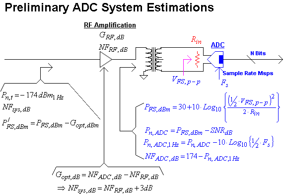
PFS,dBm = 30+10·Log10 { [ ½ · VFS, p-p ]2 / [ 2 · Rin ] } ...(1)
Most high performance ADC devices intended for RF signal acquisition offer a differential input with a maximum Full Scale "FS" peak to peak input voltage VFS,p-p and a differential input resistance Rin .This suggests a Full Scale input power limit given predicted from the previous equation(1). The ADC will exhibit a "best case" Signal To Noise Ratio (SNR) occurring near Full Scale, usually defined at PFS,dBm - 1 dB. This suggests the ADC will have an effective input noise floor given by equation (2).
Pn,ADC = PFS,dBm - SNRdB ...(2)
If the ADC were "perfect", the SNR of an ADC with a resolution of N Bits would be predicted from SNRdB = 6.02 · N + 1.76 dB. Real ADC devices never achieve this predicted limit due to imperfections. Some imperfections, e.g. clock jitter, raise the effective input noise floor of the ADC and actual measured SNR should be used instead of the theoretical limit in overall system planning. It is common to re-express the ADC's "effective resolution" in terms of "Effective Number Of Bits" or ENOB. This non integer metric is used to indicate actual resolution for comparison purposes.
Some of the ADC imperfections generate discrete spurs in addition to random noise. Again it is common practice to identify a "Spurious Free Dynamic Range" or SFDR to represent this imperfection. SFDR should not be used for Noise Figure predictions, as follows,
Pn,ADC,1Hz = Pn,ADC - 10 · Log10 { ½ · Fs } ...(3)
Random noise is assumed to be random and has a flat frequency spectrum. The ADC SNR compares an input signal at Full Scale (usually PFS,dBm - 1dB) to the total noise power integrated from 0 Hz to ½ · Fs .Equation (3) shows this total noise re-expressed in a 1 Hz bandwidth. Since Noise Figure or NFdB is defined as excess noise relative to thermal noise (at T = 298 K) the equivalent Noise Figure associated with an ADC can now be expressed as per equation (4).
NFADC = 174 + Pn,ADC,1Hz ...(4)
This NF estimate allows the preceding ADC RF amplification requirement to be determined. For example, adding excessive gain should be avoided as this will cause premature ADC overload on strong input signals. The "optimum gain" can be defined to be at the point where the total composite Noise Figure is 3 dB higher than the Noise Figure of the preceding RF amplifier stage (s) which we will define as NFRF in dB. The Optimum RF gain is therefore,
Gainopt,dB = NFADC - NFRF ...(5)
If the preceding RF amplification is less than Gainopt,dB , the overall system noise figure will deteriorate (approximately by the amount of gain reduction). On the other hand, increasing the preceding RF amplification can only reduce the overall noise figure asymptotically to the limit set by the RF amplifying stage (s), i.e. the maximum noise figure improvement can only approach, but never reach 3 dB despite how much additional amplification is added. The overall system dynamic range will however suffer as ADC overload will occur at ever reducing input levels.
The maximum system RF input level before ADC overload occurs is then,
P/FS,dBm = PFS,dBm - Gainopt,dB ...(6)
Equation (6) shows a first hand system estimation result. Other factors may suggest an alternative choice of preceding RF amplification but the use of this "rule of thumb" for an optimum gain tradeoff between overall system noise figure and dynamic range is certainly a good starting point!
Summary,
The ATMEL TS83102G0B 10 Bit, 2.2 GHz ADC appears to be a good choice for a SDR DRFSA Receiver (although the other ADC devices in the previous table also show good promise). Let's use the TS83102G0B in a "worked example".
Equations (1) to (5) predict the following, given that VFS,p-p = 500 mV, Rin = 100 Ohms, Fs = 2.2 GHz, SNRADC = 48 dB
PFS,dBm = -5 dBm
Pn,ADC = -53 dBm (To be rigorous, this is 1 dB lower given that SNRADC is measured 1 dB below Full Scale)
Pn,ADC,1Hz = -143 dBm 1Hz
NFADC = 30.6 dB
We now need to determine some probable performance parameters of the preceding RF amplifying stages. These will include some band pass filtering, required to remove unwanted alias responses from the ADC and possibly eliminate strong AM medium wave broadcast stations that may not be of interest. We will assume a fairly wide input bandwidth or 2 MHz to 960 MHz for now.
The easiest way to obtain broad bandwidth RF amplification across such a wide frequency range is to use MMIC gain blocks. These have 50 Ohm input and output terminations and relatively constant power gain. This comes at the expense of device Noise Figure, but final noise figure values around 3 to 4 dB are not unrealistic. This suggests the preceding RF amplifier power gain should be,
Gainopt,dB = 27 dB (Assumes the RF Amplifier NFRF = 3.6 dB. The final system NFsys = 6.6 dB if this value of RF power gain is selected.)
To put this in perspective, a typical conventional PMR receiver (e.g. FM, TETRA etc) will typically exhibit a Noise Figure as high as 10 dB. The suggested target of NFsys = 6.6 dB is therefore not unattractive so we will assume this performance target to be acceptable for now. Since the ADC full scale input power level was -5 dBm, the system full scale input, based on this preceding power gain of 27 dB will now be,
P/FS,dBm = -32 dBm.
For illustrative purposes, a narrow band PMR application based on analog voice FM within a 12.5 kHz channel plan will use a demodulation bandwidth in the order of 8 kHz and require a RF SNR of about 8 dB to achieve a standard reference SINAD sensitivity limit of 12 dB. The sensitivity can be predicted from,
SensitivitydBm = -174 + NFsys + 10 · Log10 {BWIF} + SNRSINAD=12 = -120.4 dBm
Compared to the predicted system full scale input this suggests a dynamic range of 88.4 dB. This dynamic range is less than provided from a well designed, conventional superhet, single channel receiver architecture (could exceed 100 dB as a "blocking" specification). It should be noted that the broad band noise floor of potential interfering signals also sets a practical upper limit usable dynamic range - e.g. an interfering transmitter with an output noise floor of 150 dB1Hz would represent a relative noise floor of -111 dB in this example IF Bandwidth of 8 kHz. Given the SNRSINAD=12 requirement of 8 dB, designed a system dynamic range higher than 111 dB - 8 = 103 dB may serve little real benefit in such a case. In other words, some additional rationale may be advisable.
A crucial difference exists between a SDR DRFSA Receiver and its conventional single channel counterpart. The conventional approach uses frequency selective filters wherever possible to restrict the danger of strong, off channel signals from overloading the receiver's demodulation sub system. This allows the following advantages,
| The narrow bandwidth filtering automatically removes the possibility of out of band overload | |
| If some "roofing" filter is applied with subsequent programmable narrow band filtering, the probability of strong signals falling inside this "roofing bandwidth" is much less than the probability of strong signals existing in a much wider reception bandwidth | |
| Multiple signals combine in a vector fashion and may result in a high peak value when all signals align in phase. Given that this is a voltage addition, the corresponding peak power amplitude can be very high for a large collection of signals with differing frequencies. Given that wide reception bandwidths will admit more potential signal channels than medium or narrow bandwidth systems, the number of potential carriers and height of corresponding power peaks is far more problematic for a SDR DRFSA Receiver than much lower bandwidth alternatives. |
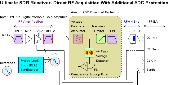
The ADC device tends to be very intolerant of signal overload. It is advisable that a signal control system is included in the signal path prior to the ADC input. This should operate only on signal peaks that could potentially overload the ADC (i.e. exceed full scale input), limiting the maximum signal level transferred. Such AGC (Automatic gain Control) is common in Single Sideband (SSB) receivers used on HF and a "fast attack, slow decay" characteristic is appropriate.
The preferred method for ADC overload protection (ADC's have very "harsh" overload characteristics compared to relatively "soft" overload in analog signal processing stages) is to place a Digital Gain Controlled Amplifier in the RF amplification sub-system as shown previously. This allows intelligent control of overall system gain rather than having a hardware imposed "fixed" limit. If additional ADC overload protection is required, the associated hardware overhead can be kept relatively minor as shown below.
The use of an AGC system will cause a "gradual" degradation in overall sensitivity when strong composite input signals exceed the receiver system's full scale input power level P/FS,dBm .The consequences of this behavior may not yet be quantified in a real field situation. If the SDR DRFSA receiver is used for spectral surveillance, occasional "desensing" on composite signal power peaks mighty only decrease reception availability from "100% of the time, all frequency channels, all at once" to "98% of the time, all frequency channels, all at once". To put this in perspective, a "scanning receiver" can be considered in comparison. If a scanning receiver was programmed for channel steps of 12.5 kHz starting at 2 MHz and up to 960 MHz, the number of scanned channels would be 76,640. Given that such a scanning receiver would capture only one channel at a time, its "availability" can never exceed 100 / 76,640 = 0.0013 % for any given channel capture. Further, if each channel capture required 100 ms for analysis (not unreasonable for a demodulation bandwidth of 8 kHz implying dt >> 1/8000 = 12.5 ms) the total scan time would become 7,640 seconds or 2.129 hours!. Clearly the SDR DRFSA Receiver has a clear and uncontestable victory in this application scenario.
I often have suggested that technology should always be matched to the application. If the application is limited by other factors, such as antenna bandwidth or multi-coupler filter bandwidth interfaces to these antennae, then the appropriate receiver bandwidth need not exceed this limitation (unless it provide other conveniences). A reduced processing bandwidth approach based on a superhet or direct conversion architecture may be better suited, and allow lower cost ADC devices with relaxed speed demands on other processing engines such as FPGAs.
Although ADC technology is continually improving, it may be some time off before a direct antenna to ADC connection is feasible. This chapter so far is intended to show both potential and limits based on what components are available today. We can guess that another 5 years may see 12 bit converters sampling at 5 GHz for example - but whether the speed of progress will be more exaggerated remains to be seen (I guess). Even so, the ENOB may still only be 8 or 9 Bits, just as the Atmel 10 Bit ADC exhibits the equivalent SNR behavior of a "ENOB = 7.6" device.
Finally, conventional technology has had significant time to mature and the exchange between technical capability and application requirement is a to-and-fro exchange of promise and need. It is not surprising that alternative receiver architectures may not "fit" markets created from this long standing interplay. Equally, new markets potentially opened and as yet not seized upon (perhaps) may forbid the use of conventional approaches. The SDR DRFSA receiver is in such a position - it can come close to conventional standards but not compete with a well engineered superhet on RF signal handling "strength" whereas the hardware intensive superhet Achilles' heal is modulation format and bandwidth inflexibility and inability to capture and process many diverse signals completely in parallel. Applications that demand the "ultimate SDR" are, as yet, still in early evolution.
Some Additional Notes:
I had thought about including some analysis of non linear behavior in addition to "dynamic range" estimations but it may be more valuable to address these issues in the following sections. Conventional "metrics" usually quantify non linearity in terms of 2nd or 3rd order "Intercept Points" either at the input of a device or system (IIP2 and IIP3) or its output (OIP2 and OIP3). The performance of high speed (Fs > 1 GHz) ADCs is still relatively poor in this regard but the issues concerned with transient overload effects that are exacerbated by having an extremely wide input acquisition bandwidth tend to dominate.
A brief mention is reasonable however; typical 2nd and 3rd order intermodulation products will be about -60 dB down on the level of two test tone signals presented at -7dBFS to a given ADC. This would correspond to IIP2 = +53 dBm and IIP3 = +23 dBm using the standard quick formula IIPm = P + dP / (m-1) where m=2, 3 etc. The OIP2 and OIP2 of the preceding RF amplifying stages should (obviously) exceed these values in order to prevent further degradation in this area. These value are not excessively high however - OIP2 performance is usually enhanced by using balanced "push-pull" arrangements and OIP3 is managed by negative feedback and "brute force" DC power input. An example MMIC with an output power capability of +17 dBm will have an OIP3 > +27 dBm, i.e. about 3 dB higher than the effective ADC IIP3 so this technical requirement is not (as yet) particularly challenging. Consequently, I decided to omit these issues for the Direct RF Signal Acquisition approach. It is currently relevant to lower speed ADC's however as these exhibit superior linearity based on current device technology.
These ADC components are potential applicants for superhet based Direct IF Signal Acquisition (DIFSA) receivers. These receivers might use an IF center frequency around up to 60 MHz based ADC over-sampling, or ~500 MHz if an appropriate alias response is used (ADC sub sampling method). These approaches are well suited to microwave SDR receivers.
If lower frequency RF reception is intended (e.g. HF below 30 MHz), these lower sampling rate converters are well suited for DRFSA receiver architectures and offer better linearity than than their higher frequency cousins identified earlier.
| Manufacturer | Device Number | Resolution
Bits |
Fs
MHz |
BW-3dB
MHz |
PinFS
dBm |
SNR @ -1dBs
dB @ [ Fin , Fs] MHz |
IM3
dB@-7 dBFs |
NFPin,SNR
dB |
ENOB @ -1dBs
[ Fin , Fs] MHz |
Jitter
ps |
DC Power
mW, [ Vs] |
| Maxim | MAX1215N | 12 | 250 | 700 | 0.81 | 65.6,[300, 250] | -86 | 28.2 | 10.6,[300,250] | 0.15 | 886, [1.8] |
| Maxim | MAX1124 | 10 | 250 | 600 | -0.12 | 56.8,[100,250] | -65 | 36.1 | 9.2,[100,250] | 0.2 | 477,[1.8,1.8] |
| National | ADC14155 | 14 | 155 | 1,100 | 4.03 | 71.3,[70,155]
66.6,[398,155] |
27.8
32.5 |
11.5,[70,155]
10.4,[398,155] |
0.08 | 967,[3.3,1.8] | |
| National | ADC12170 | 12 | 170 | 1,100 | 4.03 | 67.2,[70,170] | 31.5 | 10.8,[70,170] | 0.08 | 715,[3.3,1.8] | |
| Linear | LTC2209 | 16 | 160 | 700 | 1.53 | 74.7,[70,160]
73.5,[250,160]4 |
-105 | 21.8
23.0 |
12.1,[70,160]
11.9,[250,160] |
0.07 | 1,450,[3.3] |
| Linear | LTC2242 | 12 | 250 | 1,200 | -2.03 | 65.3,[70,250]
65.1,[240,250] |
-81
[135,140] |
25.7
25.9 |
10.6,[70,250]
10.6,[240,250] |
0.095 | 450,[2.5] |
| Analog | AD9461 | 16 | 130 | 615 | 4.03 | 76,[170,130]
74.4,[225,130] |
-89
[170,171] |
23.9 | 12.2,[170,130]
11.9,[225,130] |
0.06 | 2,200,[5,2.2] |
Note 1: This ADC has a differential input resistance Rin = 1.8 kOhm. It is not recommended to "match" directly to this relatively high impedance as such approaches will degrade third order intermodulation performance. A 200 Ohm match is preferable, achieved by placing a 225 Ohm resistor in parallel with the ADC differential input, resulting in 200 Ohms input resistance. A standard 1:4 transformer will easily interface a 50 Ohms single ended IF output stage to this defined 200 Ohms ADC differential input resistance. Since VFS,p-p = 1.385 V, the corresponding PinFS = 0.8 dBm.
Note 2: As per Note 1 with Rin = 4.3 kOhm, R/in = 200 Ohms, VFS,p-p = 1.25 V => PinFS = -0.1 dBm.
Note 3: As per Notes 1 and 2
Note 4: Both SNR results can improve if the higher input FS setting is used - also an "internal dither" option is provided. SFDR can be improved by 10 dB to -110 dB using this feature.
The superhet approach significantly relaxes the demands on ADC devices (compared to direct RF signal acquisition), FPGA signal processing and clock jitter performance. The cost savings available from lower speed components will probably outweigh any additional hardware costs associated with frequency down conversion. The drawback to Direct RF Signal Acquisition is a reduction in potential instantaneous signal acquisition bandwidth (this may be advantageous with respect to potential ADC overload).
This bandwidth reduction arises directly from the lower IF frequency compared to the RF input frequency range. In addition, the IF bandwidth must be constrained. Superhet receivers require an image reject filter prior to the frequency down conversion mixer. The performance demands on this filter increase for lower IF spectral components. Therefore, wide band IF capability creates image rejection problems for signals receiver on lower IF spectral components. This rejection difficulty exists equally for other spurious responses such as the "½ IF" mechanism as this is separated from the wanted receive frequency by only 1/2 the IF signal frequency. Further, this "front end" RF filter must accommodate the full IF bandwidth and this requirement is in conflict with its rejection requirements.
To illustrate, consider a microwave receiver intended for reception from 2.1 GHz to 2.7 GHz. A SDR DRFSA receiver could capture this entire 600 MHz "spectral chunk" and process individual signals in the digital domain. A superhet approach, in direct contrast, would face difficulties in this regard. For example, such a receiver may "suit" an IF frequency in the region of 400 MHz. Although it may appear possible to allow IF frequencies from 50 MHz to 750 MHz to reach the ADC (i.e. the complete 600 MHz spectral block), image and ½ IF rejection on lower spectral components would certainly be technically problematic. A reduced IF bandwidth would be advised, perhaps 100 MHz or so.
This limitation may not be a great detraction as receivers intended for 2.1 GHz to 2.7 GHz are most likely intended for point to point data links based on ETS 300-633 standards and frequency agility "in service" is unnecessary. However, the ability to program a receive channel frequency anywhere in this band allocation would represent a great convenience to the end user. This flexibility is easily achieved by incorporating an electronically tuned band pass filter before the first frequency down conversion mixer (e.g. Varicap tuning is relatively straightforward).
Also, the previous "surveillance" application example is not seriously compromised by the use of a superhet architecture. Reasonable pragmatic approaches include,
| Use a parallel bank of receivers spaced, in this example, at 100 MHz intervals | |
| Scan over each 100 MHz interval (6 intervals at most) and accept some loss of availability |
The superhet approach is therefore quite reasonable as a compromise to the ultimate SDR DRFSA receiver approach. We will therefore not dismiss this architecture and provide a comparison analysis with the previous DRFSA receiver.
The following "Direct Conversion" architecture may well represent a far superior approach, especially when combined with appropriate Analog IQ error estimation and correction algorithms. The demands on ADC performance are further relaxed, or alternatively, a given ADC will offer improved SNR performance at IQ frequencies centered at DC compared to frequencies centered at a high IF. Although similar ADC clock frequencies are envisaged, the available IQ bandwidth may well exceed the IF bandwidth available in a practical superhet architecture - consequently the Direct Conversion architecture may well benefit from higher sample rates than the superhet.
These ADC components are potential applicants for an Analog IQ based Direct IQ Signal Acquisition (DIQSA) for IQ signals ranging from D.C. up to ±60 MHz using an over-sampling approach. This approach relaxes the demands on the ADC performance and associated digital signal processing engine (e.g. FPGA), reduces cost but still allows wide band RF spectral acquisition when combined with an appropriate, high performance Analog RF to IQ Demodulator (Many excellent devices exist). The use of IQ error estimation and correction algorithms is essential here, as discussed in my web chapter at Rx IQ Correction - in some ways this computational procedure gets easier as the input IQ bandwidth increases!
| Manufacturer | Device Number | Resolution
Bits |
Fs
MHz |
BW-3dB
MHz |
[Vcm,VFS,p-p]
Volts, dBm |
SNR @ -1dBs
dB @ [ Fin , Fs] MHz |
IM3
dB@-7 dBFs[f1 f2] |
NFPin,SNR
dB1 |
ENOB @ -1dBs
[ Fin , Fs] MHz |
Jitter
ps |
DC Power
mW, [ Vs] |
| Maxim | MAX1219 | 12 | 210 | 800 | [0.8,1.475]
4.3@100 |
66.6,[100,210]
65.5,[200,210] |
-87
[29,31] |
31.5
32.6 |
10.8,[100,210]
10.5,[200,210] |
1,600,[1.8] | |
| National | ADC08D1020 | 8 | 1,000 | [1.26,0.65]
-2.8@100 |
46.8,[248,1000]
46.8,[498,1000] |
-50
[321,326] |
37.4 | 7.4,[498,1000] | 0.4 | 1,700,[1.9] | |
| National | ADC14DS105 | 14 | 105 | 1,000 | [1.5,2.0]
7.0@100 |
73,[10,105]
72.5.[70,105] |
<-100
[20,21] |
30.8 | 11.8
11.7 |
0.1 | 1,000,[3.3] |
| Linear | LTC2285 | 14 | 125 | 640 | [1.5,1.0/2.0]
1.0@100 |
72.4,[5,125]
72.2,[70,125] |
85
[40,41] |
26.6
26.8 |
0.2 | 790,[3] | |
| Analog | AD9640 | 14 | 150 | 650 | [1,2]
7.0@100 |
71.9,[2.3,150]
71.6,[70,150] |
85
[29,32] |
30.3
30.6 |
11.8,[2,3,150]
11.8,[70,150] |
0.1 | 750,[1.8,3.3] |
Note 1: Referenced to differential input resistance Rin (defined by an external resistor for comparison purposes)
Whilst the previous ADC applications for SDR DRFSA and DIFSA topologies can probably assume the use of transformer coupling to the ADC the Direct conversion SDR DIQSA receiver should retain DC coupling from the Analog RF to IQ converter to the ADC input. Op-Amps, or Op-Amps combined with other active devices would appear to be the most appropriate IQ amplification approach.
The IQ ADC may appear to be "voltage driven" but will in all likelihood have some series resistance added to its + and - differential inputs. A value of 50 Ohms, i.e. 100 Ohms total would not be inappropriate. This allows a quick comparison method for ADC devices based on Noise Figure "NF" and the amount of RF to IQ conversion gain, followed by IQ amplifier gain required.
The dual ADC's identified all have attractive features. The 14 Bit devices show good SNR (~72 dB) but would benefit from higher sample rates (the ADC14DS105 is only 105 MHz which limits practical IQ bandwidth capability). On the opposite side, the ADC08D1020 samples at 1000 MHz but the price paid is 8 Bit resolution. The 12 Bit MAX1219 shows a reasonable compromise and samples at 210 MHz. Although this could suggest an overall system bandwidth of BWRF = ±105 MHz, the need to reject responses on 2nd , 3rd etc alias responses requires some IQ low pass filtering. The practical IQ bandwidth is therefore a tradeoff between a percentage reduction from ±105 MHz and hardware based IQ Low Pass Filter complexity and cost. Also, I and Q BPF matching accuracy is important and most likely to interfere with spurious response rejection for signals on opposite sides of the LO carrier and especially those with offset frequencies near the LPF's upper pass-band limit.
(I have described Analog IQ error estimation and correction algorithms previously but these are intended to "fix" static I and Q errors. In principle, it should also be possible to estimate and correct frequency dependent IQ gain imbalance and phase skew errors - another idea to add to my list!)
Analog RF to IQ Demodulator IC's are available at reasonable prices (e.g. $US 4.95 @ 1,000 p.a.) but unfortunately are still somewhat "specialized" as a component variety. A few key "players" in the market include Linear Technology, Maxim-ic and Skyworksinc. National Semiconductor appears to be uninterested at this stage, whereas Analog Devices and Sirenza have not, as yet, entered the same performance field as the "top three" so far.
Analog RF to IQ demodulators can be viewed as having two distinct areas of performance availability
| Linear IQ Baseband Demodulation Accuracy - IQ DC Offset, IQ Gain Imbalance, IQ Phase Skew, RF Frequency Range, LO to RF leakage, Noise Figure, Conversion Gain (Voltage and/or power), Common Mode IQ Output Voltage Vcm , IQ Output Impedance, IQ Bandwidth. | |
| RF Input 1 dB Compression Point P1dB, Input Second and Third order intercept points IIP2 and IIP3. |
IQ errors can be estimated directly from I and Q signal statistics and shown previously. A wide band, multiple signal reception approach actually offers useful advantages. The IQ DC offset estimate becomes less affected in "DC bias" inherent in an incoming signal's modulation. For example, let's assume a (poor) FSK signal with low deviation - or even 0 Hz. This will appear similar to a carrier and if the LO is on the same frequency then the I and Q channels will have a residual DC component. The multiple channel approach forces the probability of this occurrence to be extremely low as each carrier will have a frequency offset from the LO frequency. This will ensure that subsequent integration will not be "fooled" into returning a false IQ DC offset estimate.
Similarly, the IQ DC offset can now be removed and then the I and Q channel power can be integrated. This integration can occur indefinately with multiple input channels presented to the RF to IQ demodulator, IQ amplifier and IQ ADC. Once again the danger of "bias" is removed.
Finally the "IQ phase skew" estimate can be formed after I and Q channel gains are scaled by the inverse of the previous gain imbalance estimate. This procedure is also simple - each I and Q data stream can be thought of as a vector - two vectors have a mutual angle between each other. This should be 90 degrees. The "inner product" allows this phase relationship to me estimated. Any difference from 90 degrees is the "IQ phase skew". In practical terms, dA = arcsin { (In · Qn) } is used.
Jump to this hyperlink for a demonstration / article Rx IQ Correction - I intend to expand this soon. A quick summary of the IQ error estimation and correction procedure is shown below (illustrating correction per channel if needed - remove the NCO and vector frequency shift and multiple channel correction is obtained),
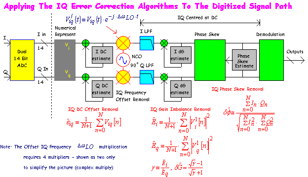
On an interesting note, signals do not need to be present for my Baseband Block based IQ error estimation (BBIQEE ?) and correction algorithm to work. RF noise is equally processed the same way as a signal would be. I have preferred to derive estimates over blocks of data, then provide updates to each correction parameter in a digital feedback loop with a parameter defined bandwidth (i.e. update speed). Low values of this parameter trade convergence speed to residual estimate variance (noise).
new_error_estimate = previous_error_estimate + ß · residual_error_estimate_after_correction
where "0 < ß <1 " represents the speed of convergence parameter or alternatively, the feedback loop bandwidth parameter. (Note: I will include another web chapter on "how to design digital IIR filters" based on a parameter defined methodology - i.e. no internal FIR is used).
Let us return now to Analog RF to IQ device comparisons. A few high performance offerings are shown in the next table,
| Manufacturer | Device Name | RF Frequency
[Min, Max] MHz |
Gain
dB, [Ohms] |
Noise Figure
dB |
Gain Imbalance
dB |
Phase Skew
Degrees |
P1dB
dBm |
IIP2
dBm |
IIP3
dBm |
Vcm
Volts |
| Linear | LT5517 | [40,900] | 3.31, [120] | 12.4 | 0.3 | 0.7 | 10.0 | 58.0 | 21.0 | 4.22 |
| Linear | LT5575 | [800, 2700] | 4.21, [130] | 12.8 | 0.04 | 0.4 | 11.2 | 54.1 | 28.0 | 3.90 |
| Maxim | MAX2021 | [750, 1200] | -9.22, [100] | 9.3 | 0.06 | 0.15 to 1.1 | >30.0
(173) |
76.0
(383) |
35.2
(223) |
0.0 |
| Maxim | MAX2022 | [1500, 2500] | -102, [43] | ?10.1 | ?0.06 | ?0.15 to 1.1 | (?173) | (51.53) | (23.33) | 0.0 |
| Skyworksinc | SKY73001 | [2, 3500] | -3.54 [500] | 17 | < ±0.3 | 1.0 | 14.5 | 70 | 25 | 1.5 |
| Skyworksinc | SKY73012 | [400, 3900] | 1.04 (-9/500) | 15.5 | < ±0.3 | < ±3.0 | 11.2 | 54, 60 | 25, 29 | 1.2 |
Note 1: Voltage Gain into a specified differential load (1 kOhm, 500 Ohms?).
Note 2: The MAX2021 and MAX2022 using a passive (bi directional) mixer approach and so have conversion loss.
Note 3: Modulator Performance for MAXIM passive IC's - indirect performance indication for demodulator performance.
Note 4: I assume this conversion voltage gain is measured with 500 Ohms differential I and Q loads. Hence Gv = 1 dB => Gp = -9 dB into 500 Ohms (from data sheet).
Although some clarification may be required for exact conversion gain conditions and impedance definitions the general performance indicators are relatively clear. However the usual mixer "Figure Of Merit" i.e. FOM = IIP3 - NF is not directly applicable here as the noise contribution from subsequent IQ amplifying stages can be extreme without careful design. It should be noted that a standard OpAmp approach may not achieve a good low noise termination to the I and Q outputs of an IQ demodulator. Also, the input common mode voltage range of any subsequent amplifier must be compatible with the average I and Q DC output voltage Vcm of the IQ demodulator IC.
To illustrate, thermal noise power at room temperature (T=298 K) is close to -174 dBm1Hz .The equivalent RMS noise voltage produced by a 50 Ohm resistor is therefore en = 0.446 nVHz . Note that the conversion voltage gains range from -3 dB to +4.2 dB (presumably < -6 dB for the Maxim devices). These low noise voltages are relatively easy to interface with at RF using devices with Noise Figures around 1 dB - but even low input noise OpAmps have input noise voltages ranging from (say) 2 nVHz (e.g. MAX4436, BW=150 MHz) to 20 nVHz . This could seriously compromise overall system noise figure and therefore require excess RF amplification to compensate. The consequence will impact detrimentally on receiver dynamic range.
Comment: The RF to IQ demodulator gain and noise figure can be used to estimate the required IQ amplifier input noise voltage requirements as follows (active versions e.g. SKY73001, SKY73012, LT5517 and LT5575)
ennV/Hz < 0.446 nVHz · 10[ ( GvdB
+ NFdB ) / 20 ]
For example, the LT5517 RF to IQ demodulator would require an IQ amplifier input referred noise voltage to be less than 2.7 nVHz to preserve the overall combined noise figure of 12.4 dB (The overall noise figure will be 3 dB higher if the IQ amplifier stages have this input referred noise voltage). The SKY73001, in comparison, would have a similar IQ amplifier input noise requirement of 2.1 nVHz .
The requirement for the passive RF to IQ demodulators (MAX2021, MAX2022) is far more stringent. The output noise voltage of these is very close to thermal noise (only increases when large input signals are present resulting from LO noise contribution) i.e. 0.446 nVHz . Consequently we observe that GvdB + NFdB ~ 0 dB. The use of a discrete IQ interface amplifier may be advised, followed by a low noise OpAmp with compatible input and output common mode voltage ranges (to suit this discrete amplifier and ADC requirement).
n order to take advantage of IQ error estimation and correction algorithms it is desirable (but not essential) to DC couple the IQ demodulator output to the ADC through intermediate amplification and filtering stages. As suggested, it may be useful to consider a discrete interface amplifier followed by a higher input noise OpAmp. The use of balanced NPN transistors can provide a low NF at low differential source impedances and can be included in an overall negative feedback loop to preserve demodulator linearity.
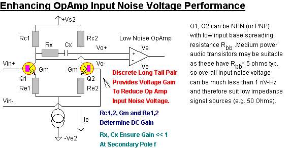
The NPN pair can be PNP but must have a low internal Rbb resistance. Medium power (1 Amp) audio power transistors are suitable providing they have reasonably high FT values (> 300 MHz) or medium FT and IC RF transistors (some care with stability may be needed when the emitters of very high FT transistors are raised above ground!).
This approach can also help interface a wide range of common mode IQ output voltages to common mode input compliance voltage ranges associated with differing OpAmps.
(Although a common emitter topology is shown, common base input stages are also feasible and often provide high input IIP3 due to a high value of inherent internal negative feedback).
It may be helpful to consider a short review on commonly available low noise, high speed OpAmps in the following comparison table,
| Manufacturer | Device Name | en
nVHz |
in
pAHz |
BW-3dB
MHz |
BWVo=1Vp-p
MHz / S.R. Vus |
Vcm (Volts)
[Vmin ,Vmax ] |
Vout (Volts)
[Vmin ,Vmax ] |
Iout
±mA |
Vs , Ve
Volts |
Is
mA |
| Maxim | MAX4223,41 | 2.0 | 20 (Vin-) | 1000, 600 | 541 / 1,700 | [1.8, 8.2] | [2.2, 7.8] | 80 | +10, 0 | 6.0 |
| Maxim | MAX4434,5,6,7 | 2.2 | 2.0 | 150 | 123 / 388 | [0, 4.0] | [0.02, 4.93] | 70 | + 5, 0 | 15.0 |
| Maxim | MAX4104,4304 | 2.1 | 3.1 | 625, 740 | 318 / 1,000 | [2.2, 9.1] | [1.3, 8.8] | 70 | +10, 0 | 20.0 |
| Linear | LTC6400-202 | 2.2 | 21.7 | 1,800 | 716 / 4,500 diff | [1, 1.6] | [0.08, 2.46] | 20 | +3, 0 | 90.0 |
| Linear | LTC6230-103 | 1.1 | 1.0 | 1450, 215 | 11, 71.6 / 35, 225 | [1.5,4] Vs=5V | [0.1, 11.9] | 45 | +12/3, 0 | 3.15 |
| Linear | LT6200,1 | 0.95 | 2.2 | 1450, 145 | 14, 108 / 44, 340 | [0, 5] Vs=5V | [0.05, 4.9] (5V) | 20 | +12/3, 0 | 20.0 |
| Analog | AD80001 | 1.6 | 26 (Vin-) | 1,500 | 1,300 / 4,100 | [1.5, 8.5] Vs=10V | [0.9, 8.1] (10V) | 100 | +4.5/12, 0 | 13.5 |
| National | LMH6624 | 0.92 | 2.3 | 1,500 | 115 / 360 | [2.0, 4.4] Vs=5V | [0.8, 4.2] (5V) | 75 | +5/12, 0 | 11.4 |
Note 1: Current Mode OpAmp - Inverting input will have highest noise current.
Note 2: The LTC6400-20 is a differential Input-Output OpAmp with a fixed voltage gain of 10:1 and differential input resistance = 200 Ohms - i.e. not well suited for the SKY73001 series IQ demodulator with 500 Ohms output resistance. Also its common mode input range is not compatible with Linear' LT5517 and LT5575 output common mode voltage of 4.22 V and 3.9 V.
Note 3: The LT6200 and LT6230-10 variants are designed for closed loop gain > 10:1. This higher closed loop voltage gain range is preferable to unity gain stable OpAmps as (a) voltage gain of about 10:1 or higher is needed to match ADC input referred noise voltage to the RF to IQ demodulator's output noise voltage and (b) unity gain approaches tend to compromise an OpAmp's output voltage slew rate and therefore its large signal bandwidth capability.
The web chapter has considered three design approaches to the Software Designed Radio receiver beginning at the antenna RF input and ending at the ADC(s) output. Issues associated with this signal path integrity have been identified so that the ability to configure "arbitrary" receiver function and performance is defined primarily in the digital domain.
Any SDR receiver places higher performance demands on its constituent components than traditional single channel, fixed bandwidth and fixed modulation format architectures. These conventional approaches are largely "hardware defined" with fixed bandwidth filters and dedicated demodulation hardware. Although alternative signal processing software could be "switched in", this would represent a large cost and complexity overhead. Further, the available hardware selection would remain fixed after manufacture.
The SDR receiver concept treats the signal path as a "transport mechanism" from the "analog world" to the "digital world". Detailed signal processing takes place after this conversion based on appropriate software algorithms. For example, multiple radio channels can be selected digitally and demodulated simultaneously. In principle these channels can all have unique and unrelated demodulation bandwidth, modulation format and bandwidth.
In practice, the "ultimate" SDR receiver can only be approached given current component technology as well as limitations we still have in our knowledge of signal processing. Both areas are progressing so the final scope of the ADR receiver is likely to remain expansive long into the future.
Hardware limitations include,
| High Dynamic Range Wide Bandwidth RF, IF or IQ signal amplification | |
| High Dynamic Range Wide Bandwidth signal digital acquisition | |
| Low jitter clock sources needed for high SNR digital acquisition |
Further the behavioral characteristics of ADC devices used for signal acquisition is different from familiar analog components. ADC devices tend to have harsh overload characteristics resulting in near complete obliteration of signals during relatively minor overload. Analog components such as amplifiers and mixers tend to have a "soft" overload characteristic so that transient overload behavior is less objectionable.
The use of a fast operating Automatic Gain Control "AGC" sub system can prevent ADC overload and result in a gradual degradation in overall receiver sensitivity when strong out of band signals cause overload conditions. However the use of a dedicated single channel receiver based on highly linear, fixed bandwidth hardware filters will always outperform a SDR receiver without such a luxury (although such filters could be switched in of course!). It is fundamental that the potential for receiver overload increases as its signal capture bandwidth increases. Two primary mechanisms exist,
| The probability of encountering a potential interfering "aggressor" is proportional to the bandwidth available for the aggressor to fall into. | |
| The peak to average ratio for multiple aggressors increases as the number of contributing channel frequencies increases. |
These limitations are independent of any particular SDR receiver architecture. It should also be appreciated that the actual receiver signal handling performance may not always be the limiting factor. For example, all transmitting sources also produce spurious outputs and noise. It may be counter productive to design a receiver's signal overload immunity to exceed the performance limitations of potentially interfering transmitting sources. Further, multiple groupings of these transmitting sources will aggravate the overall noise floor background regardless of any receiver's overload immunity.
(I raise these points not as to be an "apologist" for the SDR receiver but to place application requirements at the forefront. It is easy for people to say (I am familiar with such objections) that a receiver needs to have "strong RF performance" as "this is what the customer wants"!. Unfortunately such sentiment is unscientific and unhelpful. At the end of the day, many "customers" are associated with a given product, not just the end user. For example, a product dealer in a sales outlet may prefer to sell products that can be configured with software rather than ordered "pre tuned" from a factory, even if the end user customer will only use it on a single channel. Equally, actual observed performance in the field is the only final indication of a product's suitability for an application whereas "inferred suitability" based on personal beliefs or indirect site measurements is a poor substitute for this real world field testing with the actual product.)
Although I am all in favor of "Technology for Technology's sake" the final applications should always be matched to the technology employed. The SDR concept falls into a convenience category and also allows new applications that cannot be achieved by traditional approaches. I hope this web article helps to illustrate SDR receiver potential with a balanced analysis that also shows current limitations. These limitations may be completely acceptable; also various implementations can offset some limitations against slight reductions in software flexibility (again this matching technology-application concept!).
SDR receiver implementations fall into three main approaches
| Direct RF Signal Acquisition - DRFSA - A wide band RF input spectrum is captured digitally and processed. The only associated hardware signal processing includes low noise, high linearity amplification and anti alias rejection filters required by any continuous to discrete time sampled system. The demands on the ADC convergence are stringent - high sample rates combined with high bit resolution are at odds. Also, ADC clock jitter attacks SNR performance heavily as the input signal frequencies increase. Conventional clock and internally generated RMS jitter noise limits any ADC to an upper "effective bit resolution" regardless of how many low frequency bits may be available. For example, even 0.08 ps RMS clock jitter limits the SNR and therefore "effective bit resolution" to be SNR = 66 dB or 10.7 bits for an incoming signal frequency of 1 GHz at the ADC input. | |
| Direct IF Signal Acquisition - DIFSA - A superhet "front end" is used to translate high spectral input frequencies to lower frequencies where signal acquisition is facilitated. The IF-ADC subsystem can then be used by itself as a HF or lower VHF "DRFSA" receiver. ADC devices intended for this application have much higher bit resolution but have typical sample rates below 1 GHz. The use of "sub sampling" on a wanted higher alias response allows IF frequencies significantly higher than the ADC sample rate. The trade-off is that the overall reception bandwidth must be less than one half the clock sample rate with some additional margin. This constraint is however of some benefit in reducing the probability of IF-ADC overload. | |
| Direct IQ Signal Acquisition - DIQSA - The RF signal is directly converted to I and Q channels (usually centered at D.C. FIQ = 0 Hz with BWI = BWQ = ½ · BWRF), in contrast to approaches where a superhet front end may be included (usually to protect a "weak" IF to IQ demodulator with a preceding fixed narrow band IF filter). This "Direct Conversion" or "Zero IF" architecture has commonly been used for lower performance, low current receivers suitable for less demanding applications. The potential is far greater now that RF to IQ demodulator IC technology has advanced significantly into the realm of high dynamic range devices. RF metrics typically used to assess RF devices used in a traditional superhet receiver are now comparable - IIP3 values up to +28 dBm are not uncommon, similar to third order intermodulation performance expected from high level (+17 to +23 dBm) passive DBM mixers. |
The ability to directly acquire RF signals directly is certainly doable - additionally fast digital signal processing hardware is available for such a task. It must be realized that any receiver with in incoming signal bandwidth of 1 GHz or so must be "open season" for potentially strong signals to cause overload. Even in a relatively benign environment with a limited number of potential interfering channels, the resulting dynamic range will be in the order of 50 dB based on current ADC technology. This may be adequate for some applications but inadequate for others (e.g. would suit a fast scanning receiver but perhaps not a PMR base station).
The superhet based DIFSA receiver represents a relatively low development risk, higher performance alternative, but at the expense of some signal processing bandwidth (which may be advantageous). It can be made to equal the functional dynamic range performance of a conventional superhet when augmented with bandwidth limiting IF filters or closely approach it without. It retains a great deal of software based flexibility without a serious cost penalty (if any).
Finally the DIQSA receiver certainly has promise but may require further research before committing its architecture to a particular application. It places the lowest demands on the I and Q ADC converters as these process the lowest possible spectral frequencies ranging from 0 Hz to one half the receiver's demodulation bandwidth. It also has higher bandwidth potential than the superhet approach, and constraining this bandwidth with low pass IQ filters is somewhat easier than constraining bandwidth at a fixed IF frequency (especially if a number of "roofing bandwidth" options are considered).
The DIQSA receiver will benefit from IQ error estimation and correction algorithms - however these may not be readily available as published material. I have provided some illustration in this (and associated) web articles on how such enhancement can be achieved. The implementation need not be excessive in terms of processing overhead or complexity but sizeable performance improvement is available.
I hope this article has been illuminating. The SDR receiver (and its transmitter counterpart) is a "hot" topic these days - primarily because it is within reach of our available technologies. It may not be a "one architecture fits all" solution but then no one solution ever achieves this in any area. Flexibility always comes at some cost, but these costs need to be weighed up in actual significance compared to the application. In some ways the SDR receiver concept is one that sits on a graduated scale ranging from "zero flexibility" to "some software programmability", to "many programmable features and demodulation options" to "almost complete software configuration and control".
I guess this means that the SDR receiver and its potential applications has plenty of room to evolve and that traditional hardware defined approaches will not become obsolete overnight!
![]()
Return To: SDR
or: Ian Scotts Technology Pages
© Ian R Scott 2007 - 2008