or return to Kaleidoscope Comms
Semiconductor diodes represent in most probability the most
diverse family of devices in any component class. Although the basic
construction, in terms of semiconductor physics is basically the same, an
extremely wide range of functions and applications result from geometric detail
and material processing. The earliest "cats whisker" diodes formed by
pressing the tip of a fine tungsten wire on various crystals was used to
demodulate Amplitude Modulated (AM) radio signals for headphone reception
![]() .
.
The first patent for the cat's whisker detector was obtained in October 1906 by Greenleaf Whittier Pickard based on a crystal of silicon Si. Later, Henry Dunwoody received a patent, this time using a crystal of carborundum (silicon carbide SiC) on December 4, 1906. People experimented later on with other crystals, and inexpensive galena (lead sulphide PbS became popular around 1920.
Unfortunately this type of diode was mechanically unreliable, and the wire probe would need fine positional adjustment on a "sweet spot" of the galena crystal before adequate rectification action could occur. Even once placed, there was no guarantee that some slight bump might displace it, and the procedure of adjustment would need to be repeated.
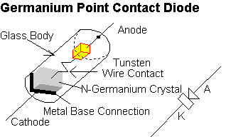
The next evolution in this "point contact diode"
was to enclose the structure in a glass cylinder, preventing subsequent
movement. Galena crystal was replaced with a crystal of germanium Ge, mounted on a
metal base. A thin tungsten wire was then pressed into the crystal, forming a
reliable point contact diode
![]() , suitable
for mass production.
, suitable
for mass production.
Point contact diodes were widely used for AM detection of
radio waves, and the small contact area resulted in very low self capacitance,
thereby allowing high frequency operation even up to frequencies of several GHz
![]() .They were still a
mechanically formed process, and required careful assemble, and a post assembly
electrical "forming" process in which a current was used to help
establish a useful junction. In addition, the small junction area limited the
amount of current that could flow through them, without damage, usually only a
few mA.
.They were still a
mechanically formed process, and required careful assemble, and a post assembly
electrical "forming" process in which a current was used to help
establish a useful junction. In addition, the small junction area limited the
amount of current that could flow through them, without damage, usually only a
few mA.
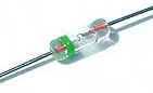
Physical appearance of a typical glass cased germanium point contact diode
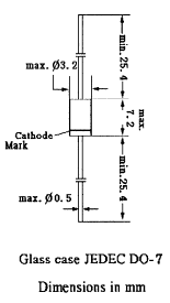
Typical dimensions for these glass point contact diodes
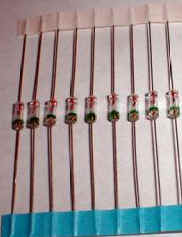
Multiple germanium point contact diodes on a paper guide
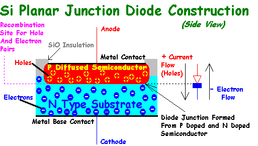
The next step was to generate a chemical process for junction formation, which can be represented as a marriage between two distinct semiconductor versions based on added impurities, referred to a "N-Type" and "P-Type". This was first demonstrated by Russell Ohl in 1940 when he demonstrated the P-N junction to his employer. The N-Type is doped with an impurity that creates an excess of free electrons in the material, whilst P-Type has a relative absence of electrons or "holes". This process was first used for germanium junction diodes, but subsequently became dominant with silicon.
Typical semiconductors and their dopant elements can be identified in the following table,
Truncated Periodic Table on Period / Row, Atomic Number
|
Period Row |
III-A 13 |
IV-A 14 |
V-A 15 |
Advantages of IVA (14) Semiconductor | Usage |
| 2 | B Boron 5 | C Carbon 6 | N Nitrogen 7 | Very-High Temperature SiC = carborundum | Future semiconductor, SiC recently used in high power Schottky diodes (Infineon) |
| 3 | Al Aluminium 13 | Si Silicon 14 | P Phosphorous 15 | High Temperature, Cheap | Silicon is the most common semiconductor today |
| 4 | Ga Gallium 31 | Ge Germanium 32 | As Arsenic 33 | Ge is now used as SiGe Hybrid, best frequency transistor performance |
Ge is obsolete when used by itself, due to poor high temperature performance. |
| 5 | In Indium 49 | Sn Tin 50 | Sb Antimony 51 | Sb used for infrared detectors | |
| 6 | Tl Thallium 81 | Pb Lead 82 | Bi Bismuth 83 | Galena=PbS + cats-whisker) Sulphur 16 | X-Shield |
| Donor Type | P-Type dopant | Intrinsic Semiconductor | N-Type dopant | Dopants are added by heated vapor deposition, or direct ion implantation, especially arsenic As |
Dopants are usually adjacent to the
semiconductor in the periodic table, but some exceptions occur, e.g. galena PbS.
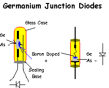
Typical early construction and encapsulation for Germanium Ge junction diode variants.
Germanium junction diodes were initially produced but were soon replaced with Silicon Si versions, due primarily from advances in chemical processes required to produce extremely pure silicon wafers.
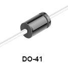
Typical leaded (DO-41) 1 Amp Silicon junction rectifier diode appearance (example 1N4007).
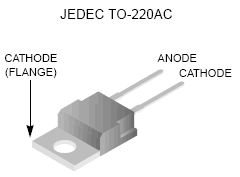
Higher current chassis mounted (TO-220) 10 Amp Silicon junction rectifier diode appearance
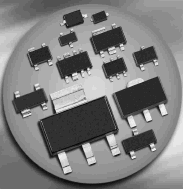
Assorted SMD Case styles for single and multiple Silicon diodes (Infineon graphic)
To understand the operation of a semiconductor diode , consider the following circuit diagram,
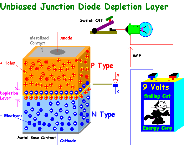
When the switch is in its "off" position, the N-Type material has an excess of electrons, and the P-Type material has an excess of holes. At the junction of the two, some holes migrate into the N-Type material and some electrons migrate into the P-Type material, create a thin layer of charge inversion. This represents a state of equilibrium. Now lets close the switch.
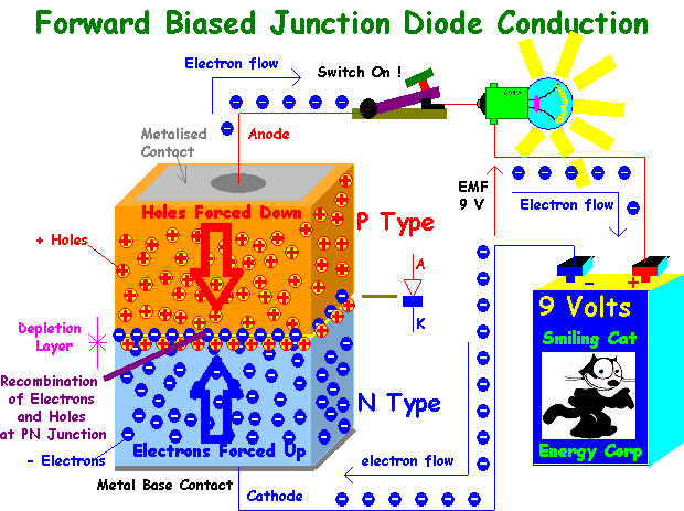
Now the N-Type material obtains a negative potential from the negative (-) terminal of the battery, and so its negatively charged electrons experience a force that pushes them upwards. Equally, the P-Type material obtains a positive charge from the positive potential (+) of the battery, and so the positively charged holes are forced downwards.
These charges meet at the junction, and "recombine" allowing a net current flow, as can be seen by the glowing light bulb.
One way to understand recombination, is to consider a simple analogy,
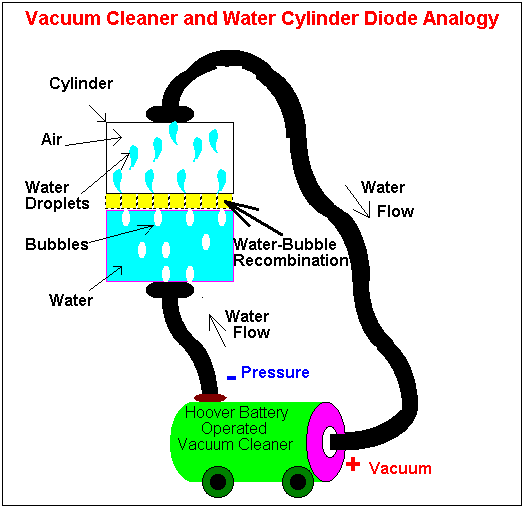
Let's imagine the vacuum cleaner to be the same as the battery, as an energy source. By creating a vacuum at its front (positive terminal), it will try to attract the water droplets (electrons) inside. Equally its exhaust opening (negative terminal) will create a pressure that will force the water inside the container upwards. If enough force is applied, this pressure will force some small water droplets through the thin porous membrane shown (junction) and emerge as water droplets that fly upwards. These will be collected in the vacuum cleaner's pipe and flow into its front.
These get spun through its motor drive propeller and flow immediately out its exhaust, completing the circuit.
However, notice what happens at the porous membrane. For each water droplet that flows up, a bubble will form directly under its departure. These bubbles (holes) will whiz everywhere, just like a fizzy drink. This represents recombination.
You could equally imagine it upside down, for each falling droplet, a bubble would form above it.
Of course no analogy is ever perfect, and the apparatus above would not demonstrate the diode's ability to block the flow of current in the reverse direction. This requires a study of semiconductor physics.
Click on this link to find out more on semiconductor diode
equations
As mentioned, junction diodes have great variation in construction, operation and application, more that than any other component. Semiconductor junctions are actually easily formed, and by 1927 LO Grondahl and PH Geigerpeople discovered that simple stacks of iron and copper disks could be pressed together to form a high current, but slow diode suitable for cat battery chargers (although small low capacitance versions were used in multi-meters and could operate to about 1 MHz!). At the time these copper oxide rectifiers were cheap and reasonably reliable.
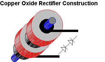
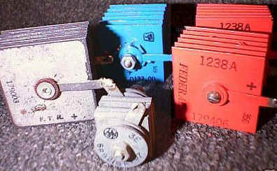
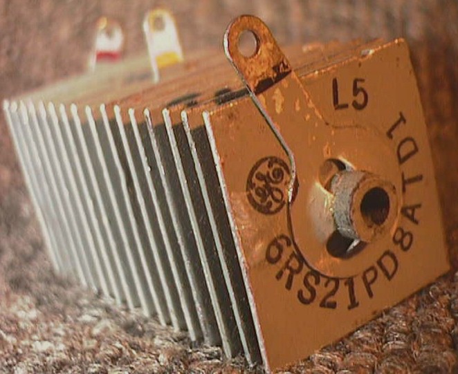
Typical physical appearance of copper oxide rectifier diodes
These rectifier diodes could withstand 10 Amps of current and were tolerant of temporary overload, as in the case of shorted battery charger cables. They were not able to withstand high reverse voltages however (about 6 Volts maximum), hence the need to stack many disks in series even for a 12 Volt battery charger. This created a larger forward voltage drop and consequently their rectification efficiency was poor.
Other materials were tried, based on similar principles.1933 by C.E. Fitts
invented the Selenium rectifier which could withstand much higher voltages (20
to 30 Volts), and still operate at high current
 .
.
These new rectifiers became popular replacements for high voltage vacuum tube rectifiers used in valve radios, and were smaller and more efficient, but still based on a stacked cell approach. Typical rectified output voltages ranged from 110 Volts to 250 Volts, depending on the radio's design.
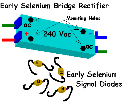
Later, small signal diodes were also manufactured, suitable for audio applications but limited to frequencies less than 500 kHz.
These early 1940's or so diodes were useful for power applications, but not for radio frequencies. The point contact diode was excellent, but unfortunately the junction diode was somewhat dismal when it came to speed. Unfortunately, recombination is a slow process, a bit like waiting for a car to pull out from its park, leaving a space you can then drive in to. You wouldn't do this maneuver at 100 km/hour I guess.
The solution was invented by Walter Schottky, with publications around 1938, simply by removing one of the junctions and replacing it with a metal contact. This removed holes, and therefore recombination delay was eliminated. It turned out that the same diode action occurred, but with about ½ the forward voltage drop of the junction diodes.
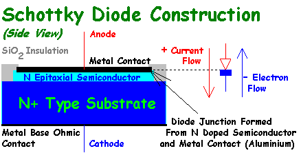
Schottky diodes allow efficient RF detection or rectification beyond several GHz, even in standard SMD packages. They are also used as high efficiency rectifiers in "switch-mode power supplies" that require the diode to rectify frequencies as high as several MHz, also at many amps of current. One weakness is that they have lower breakdown voltages than their junction diode counterparts. The highly successful "1N4007" 1 Amp junction diode can support 1000 Volts in the reverse direction. In contrast, a Schottky diode reverse blocking capability ranges from a few volts (microwave diodes) to about 70 Volts.
So far we have emphasized the diode's importance as a
rectifier, i.e. to convert AC to DC. There is a version of diode called a
Varicap, or "Variable Capacitance Diode" that is used exclusively in
the reverse direction as a variable capacitor
![]() . The Varicap diodes have the same basic structure as the junction diode,
but the doping profile next to the junction is specifically designed. The area
of the junction, combined with the dielectric constant of the semiconductor and
the distance of the depletion layer forms a capacitor. In forward bias, this
layer diminishes to allow recombination. When reverse biased, the opposite
charged pairs at the junction are pulled apart, and the effective distance is
determined by the applied voltage. The degree of variation in capacitance
depends on the doping profile, variations of 3:1 on capacitance are typical of
most junction diodes, at 7:1 the diodes become "abrupt junction"
versions, at 12:1 or more they will be "hyper abrupt" types.
. The Varicap diodes have the same basic structure as the junction diode,
but the doping profile next to the junction is specifically designed. The area
of the junction, combined with the dielectric constant of the semiconductor and
the distance of the depletion layer forms a capacitor. In forward bias, this
layer diminishes to allow recombination. When reverse biased, the opposite
charged pairs at the junction are pulled apart, and the effective distance is
determined by the applied voltage. The degree of variation in capacitance
depends on the doping profile, variations of 3:1 on capacitance are typical of
most junction diodes, at 7:1 the diodes become "abrupt junction"
versions, at 12:1 or more they will be "hyper abrupt" types.
Varicap diodes are used in car radios, TV tuners and many industrial applications where frequency control of a resonant circuit is needed from a DC control voltage. Being reverse biased, little if any current is needed for this control. Without Varicap diodes, programmable channel selection on radio's and TV's would require a mechanical solution, and would probably be expensive or impractical.
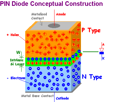
Still this does not exhaust the diode family of members. Yet another class, called a PIN, or P-Type, Intrinsic, N-Type is designed with a middle layer of un-doped material between the P and N types. This modification purposely exploits recombination time in order to prevent rectification of RF signals. The intrinsic layer traps charges, prolonging their lifetime. Such diodes are used as DC current controlled RF resistors. The suppressed rectification behavior allows low distortion in circuits designed to control RF signal levels, based on a forward biased current flow.
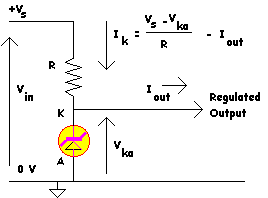
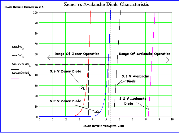
So far we have seen rectification, controlled capacitance and controlled resistance, all in AC applications. Still, many other diodes are designed for DC applications. For example zener diodes are designed to have a controlled reverse voltage breakdown characteristic and are used for voltage regulation. Voltage ranges fro a few volts up to 5 volts actually use the zener phenomena, whilst those from 5.5 volts to 50 volts or so are more accurately referred to as avalanche diodes. Avalanche diodes maintain an accurate reverse voltage over a wide range of reverse currents. Zener diodes, in contrast, have a much softer "knee" in their characteristic, but both have applications in voltage regulation.
At the beginning of the article, we mentioned the use of
incandescent lamps for indicators on equipment. Light Emitting Diodes (LED)
![]() are now used as
longer life alternatives, and come in red, green, yellow and blue colors. (The
LED phenomenon was first reported in 1907 by H.J. Round, who found that various colors
could be produced from a crystal or carborundum, i.e. silicon carbide when
voltages between 10 volts and 100 volts were applied). Recent
high luminosity versions are even used for house lamps. Other versions on the
theme create Laser diodes.
are now used as
longer life alternatives, and come in red, green, yellow and blue colors. (The
LED phenomenon was first reported in 1907 by H.J. Round, who found that various colors
could be produced from a crystal or carborundum, i.e. silicon carbide when
voltages between 10 volts and 100 volts were applied). Recent
high luminosity versions are even used for house lamps. Other versions on the
theme create Laser diodes.
The reciprocal light-electronic conversion diode devices
include photodiodes
![]() and solar panels.
and solar panels.
In summary diodes cover the following wide range of applications
| Diode Family | Time Frame | Construction | Application |
| Cat's Whisker | 1906 | SiC, Si, Galena with tungsten wire on "sweet spot" | AM radio reception |
| Point Contact | Subsequent improvement | Germanium with tungsten wire, usually housed in glass. | AM reception, microwave detection |
| Copper Oxide | 1927 | Stacked Copper oxide and Iron disks on a bolt | High current battery charger |
| Selenium | 1933 | Stacked Selenium and metal deposits. | High Voltage rectifier, battery charger |
| Junction Diode | 1940 | Silicon or Germanium, Chemical deposition of impurities | General purpose, computer diode |
| Schottky Diode | 1938 | N-Type Silicon and metal deposition | High frequency detection, high speed high power rectification |
| Varicap Diode | Junction Diode, doping profile | Voltage controlled tuning | |
| PIN Diode | Junction diode with intrinsic layer | Current controlled attenuation | |
| Zener Diode | Junction diode, doping profile | Voltage regulation, clamping | |
| Light Emitting Diode | Junction Diode, exposed junction | Indicator lamp, house lighting | |
| Photo Diode | Junction Diode, exposed junction | Light detection, LED-optical isolation | |
| Solar Cell | Junction Diode, Wide Area | Solar electrical power generation | |
| Tunnel diode | highly doped junction diode | not mentioned, u-wave oscillators | |
| Impatt diodes | Not really a diode, no junction | not mentioned, u-wave oscillators | |
| Step Recovery Diode | Junction Diode, processed for high frequency with charge storage in junction | not mentioned - Uses recombination charge to create sharp snap off pulse for harmonic generation at microwaves | |
| Diacs | Not really a diode | not mentioned - fires Triac devices |
This comes to an impressive 16 categories and applications, some of which span power levels from less than Pico-watts up to Kilo-watts.
Return to A Component Universe
or return to Kaleidoscope Comms