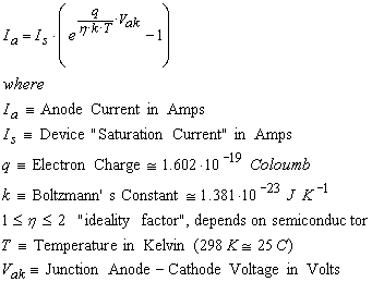
 ...(1)
or return to ACU Semiconductor Diodes
All electronic components benefit from equations that describe some aspect of their behavior. Semiconductor diodes are no exception, and have many V-I characteristics suitable for analysis.
These electrical relationships can be separated into two main categories, DC or static behavior and AC or dynamic behavior. When operating frequencies associated with AC behavior become sufficiently high so that package parasitic effects become significant, for example case capacitance, lead inductance, it is usually to refer to these AC characteristics as RF (Radio Frequency) behavior.
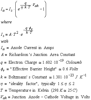
Semiconductor diodes all exhibit an exponential relationship between device current and applied voltage,
...(1)
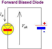
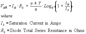
Equation (1) applies equally for forward (conducting) bias as well as reverse (blocking) bias. The voltage Vak applied between anode and cathode terminals and the resulting anode current Ia are both defined as positive quantities for forward bias and negative quantities for reverse bias.
Equation (1) has many fixed coefficients that can be lumped into a single constant,
 ...(2)
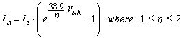
We note that Ia = 0 when Vak = 0, and that Ia -> -Is when Vak -> -infinity. Relatively small Silicon junction diodes with maximum currents in the order of 100 mA or so will have a saturation current Is ~ 10-10 Amps, larger junction diodes will have higher saturation currents. It may be instructive to consider a table of predictions for diode anode current Ia for different applied forward bias voltages Vak and diode coefficients, Is and the ideality factor.
| Vak
Volts |
Is
Amps |
Ideality Factor | Resulting Ia
Amps |
Comments and Observations |
| 0.6 | 10-10 | 1.5 | 5.7 · 10-4 | Small signal diode, 0.57 mA forward current will flow at this bias voltage |
| 0.7 | 10-10 | 1.5 | 7.7 · 10-3 | Small signal diode, 7.7 mA forward current will flow at this bias voltage |
| 0.8 | 10-10 | 1.5 | 1.0 · 10-1 | Small signal diode, 100 mA forward current will flow at this bias voltage |
| 0.7 | 10-10 | 1.0 | 6.7 · 101 | If the semiconductor was "perfect" it would conduct 67 Amps! |
| 0.7 | 10-10 | 2.0 | 8.2 · 10-5 | If the electron and hole pairs are less available, then 82 uA will flow! |
| 0.5 | 10-8 | 1.5 | 4.3 · 10-3 | A large junction diode, like many in parallel, has high current at low bias |
Note: This "ideality factor" has a strong effect on forward conduction. Germanium has the best ideality factor ~ 1.1 or so, whereas Silicon is between 1.1 ~ 1.5.
As we see, a forward bias around 0.7 Volts tends to result in reasonable currents for small signal electronics. Unlike some text claims, there is no "knee" where conduction occurs, as the transfer characteristic is exponential everywhere. Conduction, per se, is just a matter of scale.
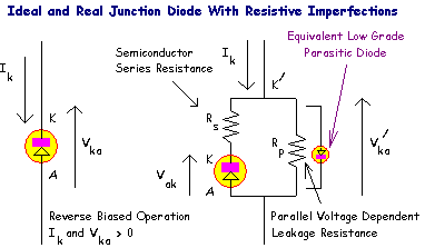
All diodes have some finite series resistance caused by the resistivity of semiconductor material between the active junction and their connecting terminals, (which add some smaller amount of additional resistance also). This additional resistance is approximately constant with current, leading to the following model,
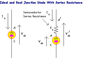
Unfortunately, no closed form solution exists for anode current Ia as a function of anode-cathode voltage Vak , however Vak can be made the subject with little difficulty, since the final diode forward bias voltage V/ak will equal the original predicted diode forward voltage Vak added to the voltage drop across its additional series resistance VRs = Ia · Rs .
 ...(3)
This addition series resistance varies from diode to diode. Modern small signal Silicon junction diodes will have values of Rs ~ 5 Ohms, Large rectifier diodes will have much lower values, e.g. Rs ~ 0.1 Ohms. In comparison, a typical Germanium point contact diode will have much higher series resistance, typically Rs ~ 300 Ohms.
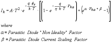
Real diodes also suffer from additional parallel leakage current paths that become most apparent when operated in reverse bias. This parallel resistance causes significant additional current when the diode is reverse biased, since currents in this blocking mode are sufficiently low to reveal them. Further, this resistance is voltage and temperature dependent.
 ...(4)
This time we see that the saturation current Is has a strong temperature dependence, far more so than current variation caused by the exponential term (which competes with an increase in current as temperature increases). What is also interesting is that the this leakage current mechanism actually behaves like a reverse biased, very low grade parasitic diode.
When moderately reverse biased, the effect of the series resistance term Rs will be negligible, due to the low expected current flow. We will propose the following diode model intended for best accuracy in the reverse biased region (note we will use Ik instead of Ia just to preserve a convenient sign convention),
 ...(5)
Equation (5) now describes the voltage dependent leakage current that is typically observed in real Junction diodes. Reverse biased behavior behaves similarly to the forward biased characteristic, but has a much higher apparent “threshold” voltage, as expected from a low grade parasitic diode. The second added exponential term accounts for the current contribution from this unwanted “parasitic” diode.
When a reverse voltage is applied to a semiconductor, electrons are attracted towards the positive terminal and holes are attracted towards the negative terminal. This drift velocity is very slow, compared to walking for example, but on an atomic level it can become hectic. These drifting charges will sometime collide with atoms and release additional charges. Usually the atoms will have enough attractive charge to return these charges to equilibrium. However, as the voltage is increased, the force exerted on these charges reaches a point where it exceeds the attractive force of the host atom and the charges are ripped away. This causes an abrupt increase in current, referred to as an avalanche current.
This effect can be idealized as a sharp threshold of reverse conduction, tamed down by some additional voltage drop caused by semiconductor series resistance.
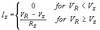 ...(6)
When the applied reverse voltage VR is less than this threshold voltage Vz then practically no reverse current Iz flows. However, when Vz is exceeded, the resulting current is limited only by this series resistance Rz .
As mentioned in the previous web page, "Zener" diode is used historically for both Zener diodes and avalanche diodes. Zener phenomena is prevalent for voltages less than about 5.5 Volts and has an exponential characteristic, avalanche behavior occurs in diodes above 5.5 Volts, and is abrupt. For voltages near this limit, both mechanisms add in parallel.
Varicap diodes are used for voltage tuned filters and also for resonators used in Voltage Controlled Oscillators (VCO). The available frequency tuning range depends on the amount of capacitance variation that the diode can provide. The standard Varicap diode transfer equation is
![]() ...(7)
...(7)
Cv
represents the Varicap diode capacitance for a reverse bias voltage v,
Cp represents a stray parallel capacitance, C0 represents
a capacitance coefficient, Ø represents a voltage offset around 0.7 Volts, and
![]() represents a "grading coefficient". Varicap diodes typically provide
capacitance values between 1 pF and 100 pF, although some special versions
provide as much as 600 pF of capacitance and are used in medium wave car radio
tuners. The amount of capacitance variation depends on the grading coefficient,
values around 0.3 occur in standard junction diodes and cause 1:3 ratio, abrupt
types have larger grading coefficients with about 5:1 capacitance ratio,
while hyper abrupt types provide over 10:1 capacitance ratio.
These enhanced abrupt and hyper abrupt Varicap diodes are created by careful
control of the doping profile around the active semiconductor junction.
represents a "grading coefficient". Varicap diodes typically provide
capacitance values between 1 pF and 100 pF, although some special versions
provide as much as 600 pF of capacitance and are used in medium wave car radio
tuners. The amount of capacitance variation depends on the grading coefficient,
values around 0.3 occur in standard junction diodes and cause 1:3 ratio, abrupt
types have larger grading coefficients with about 5:1 capacitance ratio,
while hyper abrupt types provide over 10:1 capacitance ratio.
These enhanced abrupt and hyper abrupt Varicap diodes are created by careful
control of the doping profile around the active semiconductor junction.
It
might be thought that high capacitance ratio diodes would always be best, but
this is not necessarily the case. Varicap diodes manufactured for high
capacitance ratios tend to have much higher series resistance Rs
than those with softer doping profiles (low ratio). The Quality Factor or Q of
the Varicap diode is inversely proportional to this series resistance.
Consequently, the optimum choice of
diode is not clear-cut. In many applications, the available Varicap diode capacitance
ratio is
far greater than required, but can be “watered down” by the inclusion of a small
series capacitance Cs
.

If a Varicap diode is placed directly across an inductor, the resonant frequency ratio f2 / f1 will be proportional to the square root of the capacitance ratio, i.e. f2 / f1 = [Cv1 / Cv2 ]-½ where we will consider f2 > f1 so that Cv1 < Cv2 (i.e. the frequency will increase as the diode reverse voltage increases, reducing its capacitance). For convenience we will use angular frequency w from now on defined as w = 2 · pi · f .
The value of series capacitance Cs can be determined from the minimum required resonant frequency w1 , the maximum resonant frequency w2 , the maximum Varicap diode capacitance Cv1 at reverse bias voltage V1 , and the minimum Varicap diode capacitance Cv2 at bias voltage V2 .
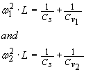 …(8)
…(8)
Eliminating Cs and making L the subject,
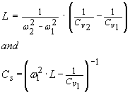 …(9)
…(9)
This procedure allows us to determine the external component values, although parallel capacitance can also be added we will consider the simplest case first, in order to find a Figure of Merit for the Varicap diode. This is necessary because Varicap diodes with wide tuning ratios tend to have a high series resistance, and therefore a relatively low component Q. However this reduced Q is offset by the ability to use a smaller coupling capacitor Cs which tends to offset this reduced Q characteristic. The question now is which is best? A Varicap diode with high component Q and "tight" coupling, or a hyper abrupt Varicap diode with lower Q but a high tuning ratio, and "loose" coupling? The analysis that follows will provide some insight into this trade-off.
Having determined L and Cs we will need to know how the Varicap diode series resistance Rs affects the overall circuit Q. The Varicap diode Qd can be defined as,
![]() …(10)
…(10)
It can be seen that the Varicap
diode Qv
reduces as the operating frequency
w
increases, or as the Varicap diode
capacitance Cv increases (i.e. as the reverse bias
voltage V
is reduced). In any given tuned
circuit, the resonant frequency is inversely proportional to the square root of
the total tuning capacitance, but the resonant frequency is directly
proportional to capacitance. The overall Qv therefore increases with resonant
frequency in a given circuit with fixed inductance. The worst case
Qv
therefore occurs at the lowest bias
voltage and corresponding resonant frequency. We will define this Qv,min
condition as
![]() …(11)
…(11)
The overall minimum circuit Q also
occurs at the lowest tuned frequency as,
![]() …(12)
…(12)
Combining equations (9) and (11)
and (12) now suggests that,
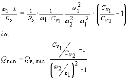 …(13)
…(13)
Equation (13) now provides direct insight into a given Varicap diodes impact on the worst case circuit Q based on the lowest tuned frequency w1 , the relative tuning frequency range w2 / w1 , its available tuning capacitance ratio Cv1 / Cv2 and its minimum Qv, min .
A suitable Varicap diode Figure of Merit FOMQ for a given frequency can now be defined as,
![]() …(14)
…(14)
Since ![]() we
now define FOMQ as a frequency independent parameter where Cmax
is defined as Cv1 and the frequency term is simply omitted, as
it would be the same value for any comparison between competing Varicap diodes.
This suggests,
we
now define FOMQ as a frequency independent parameter where Cmax
is defined as Cv1 and the frequency term is simply omitted, as
it would be the same value for any comparison between competing Varicap diodes.
This suggests,
![]() ...(15)
...(15)
This is a curious result, since Cmax will be many times greater than Cmin for many Varicap diodes. This suggests that, as a first approximation, Varicap diodes with the lowest product Rs · Cmin will have the highest figure of merit.
Silicon Varicap diodes have benefited from a great deal of Research in recent years and continually push the envelope in terms of their effective FOMQ .
Holes and Electrons require a certain time to “pass through” each other at the P-N Junction. This time T is called “recombination time”. This means that there will be a corresponding time delay in a previously forward biased diode’s ability to block current flow after it is switched into reverse voltage. Consequently we would expect an upper frequency limit to AC to DC rectification when T becomes equal to one half the AC time period, i.e.
![]() …(16)
…(16)
Rectification efficiency can be expected to decline quickly for frequencies above this upper threshold.
Current high speed P-N junction diodes have “turn off” times in the order of 2 ns at moderate forward bias currents. From equation (16), the diminished rectification frequency threshold would then correspond to 250 MHz. This is not a clear-cut limit, and AC to DC power conversion efficiency will fall off at much lower frequencies, and can still allow rectification at much higher frequencies.
The effect of this charge storage is
analogous to having a current dependant capacitance placed across the junction.
The total charge Q stored in the junction will depend on the forward current flowing and the time
T required for carrier recombination,
![]() …(17)
…(17)
Since the charge
stored in a capacitor is Q = C · Vak
then we can imply a current
dependent junction capacitance of,
![]() …(18)
…(18)
As an example, a typical
P-N
junction diode (1N4148, BAV70 etc) may have a typical zero bias junction
capacitance of only 2 pF. These diodes have a typical turn off or
recombination time in the order of T = 2
ns. Equation
(18) predicts an
effective forward biased junction capacitance of 286 pF, at a forward bias
current of 100 mA, assuming a forward voltage drop of Vak ~ 0.7
Volts.
Certain diodes make use of this
property. PIN diodes, for example, have a thin intrinsic semiconductor layer
placed in-between the P-N junction. This traps charge, and has the effect of inhibiting diode
rectification but still allows the effective forward biased (incremental or AC)
resistance to be controlled by a forward bias current. This property is useful
in current controlled attenuation circuits. The inhibited rectification behavior
allows large RF currents to be controlled by smaller DC forward bias currents
without distortion. Another version of the above is referred to as a “Band
Switch Diode”. The PIN diode usually has an AC resistance rd
that closely follows,
![]() …(19)
…(19)
The resistance scale term R0 ~ 25 Ohms when Iak is expressed in mA, but varies from PIN diode to PIN diode.. Low values of series resistance, as might be wanted in a RF switch would require high forward bias currents that could be unattractive. The “Band Switch Diode” attempts to place its charge dependent capacitance in parallel with rd , effectively “shorting it out”, especially at high frequencies. This allows very low “on resistance” at bias currents as low as 1 mA. The two types of diodes can be identified by their frequency behavior. Standard PIN diodes have a constant rd with frequency, whilst Band Switch (PIN) diodes show a combined rd that falls sharply as frequency increases.
As mentioned, the term "RF" tends to become appropriate when the package parasitic effects of a component start to show their importance. In the case of a junction diode, its terminals will have a finite series inductance, which can be several nH even for short lengths. High frequency applications, for example at frequencies greater than 100 MHz, may need to include these extra effects.
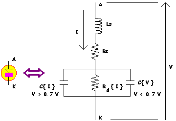
In addition to parasitic effects, semiconductor junction (and point contact) diodes also exhibit non linear effects. In the case of Varicap and PIN diodes these non linearity's cause unwanted Intermodulation distortions, but some non linearity can be used to advantage, for example in AM demodulator circuits.
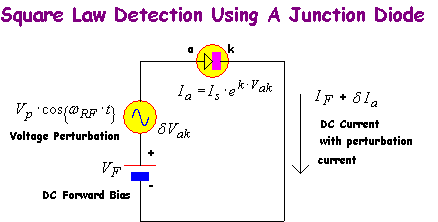
In many cases it is useful to know the incremental current and or voltage behavior of a given component so that its small signal, low frequency characteristics can be ascertained. This analysis is usually provided for the forward bias case, with some realistic simplification.
![]() …(21) (Defined simply for the
purpose of this analysis)
…(21) (Defined simply for the
purpose of this analysis)
Differentiating with respect to voltage we find,
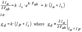 …(22)
…(22)
The forward biased diode’s “dynamic conductance” gd is closely proportional to the junction diode’s forward bias current IF given that the saturation term will generally be small and since resistance is defined as the reciprocal of conductance we can also state,
![]() …(6)
…(6)
The junction diode can now be seen to provide a current dependent conductance and therefore a current dependant resistance also. This assumes that the current perturbations are small compared to the diode’s forward bias current of course.. We can also gain some insight into its non- linear properties in the forward bias region by expanding equation (4) as a Taylor series,
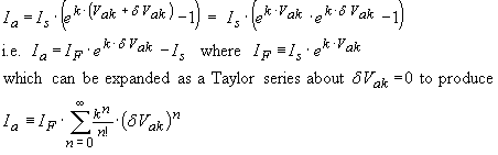 …(7)
…(7)
In this case
![]() represents a small perturbation in
voltage around a given forward bias voltage VF
. Also note the n=0 term corresponds to the diode’s DC bias current, the n=1
tern corresponds to the previous expression for the dynamic conductance
gd
and the n=2 term is of interest for
small signal detection and frequency mixing. In this case
represents a small perturbation in
voltage around a given forward bias voltage VF
. Also note the n=0 term corresponds to the diode’s DC bias current, the n=1
tern corresponds to the previous expression for the dynamic conductance
gd
and the n=2 term is of interest for
small signal detection and frequency mixing. In this case
![]() …(8)
…(8)
From equation (8)
![]() , therefore,
, therefore,
 …(9)
…(9)
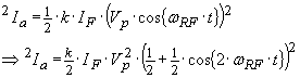
The average current can be found by integrating equation (9) over a complete cycle, to produce
![]()
Jump to some MATHCAD files showing diode coefficient
extraction ?
Or return to ACU Semiconductor Diodes