![]()
The semiconductor age has revolutionised electronics with miniaturised circuits performing convenient, advanced signal processing functions. Semiconductor devices are used for power electronics, audio amplification, radio frequency amplification, optical processing and digital computations.


Prior to this we lived in a land of wires, relays, twine and sealing wax. Even the emergence of de Forest’s vacuum tube belonged to an era of hand-connected components mounted on bent, drilled and machined metal chassis bolted into equally hand crafted wooded cabinets. Although nostalgic to some, individual production of such expensive items was never an ambition of the industrial revolution. Mass production, based on repetitive tasks, each being a sub component of the whole, was the enviable position to be attained. Towards this end we saw the use of PCB substrates supporting leaded components and socket held valves, each searing their surroundings with heat for the purpose of relatively simple signal processing.
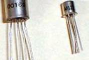
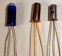
The semiconductor promise was one of reduced size and heat, both of which beckoned more complex signal processing tasks to be performed. As the number of semiconductor components increased, reliability issues became increasingly important. Anecdotal stories of house sized computers built with vacuum tubes serviced by teams of technicians repairing defects every few hours are easily found. The translation to transistors, at first based on at least one occasion by the “point contact” germanium transistor improved this situation considerably. The grand centre stage show belongs to the invention of the integrated circuit, for which the photographic process used for device definition and interconnection has become tuned to a fine art. Resolutions available today parade themselves at a fraction of the wavelength of light used for creating the lithographic screens used for device fabrication. Complexity, Heat and Reliability issues are now replaced by those associated with Software Reliability.
Semiconductors had shown non linear properties such as rectification up to this point in time, but the domain of signal amplification belonged to the vacuum tube triode, tetrode and later the pentode. The vacuum devices had evolved significantly with time, and became small enough to operate as hearing aid amplifiers and operate from voltages as low as 9 Volts. They still required a heated (red) hot cathode filament, which only served to waste energy and shorten battery life.
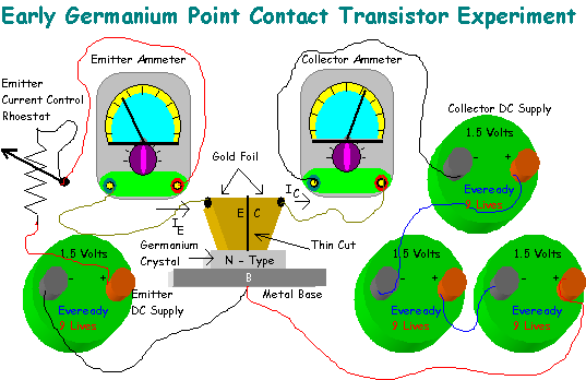
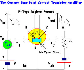
The idea of a “solid state” amplifying device remained elusive until Schottky and his team at Bell labs finally resolved previous failed attempts at semiconductor based amplification. The structure they invented was based on a single Germanium crystal mounted on a metal electrode with two closely spaced gold metal strips pressed on to its surface. These formed the “Emitter” and “Collector” terminals, and the metal mounting plate formed the “Base”.

This early experimental transistor had a
common base current gain of about 2, and although this was a very low value of
amplification even by the standards of the time, in was nonetheless evidence of
amplification potential. Commercial interest in manufacturable devices followed
immediately, and many experimental “point contact” germanium devices were
produced. These used a similar construction to their point contact diode
predecessors, but were difficult to manufacture as the two wire “whiskers”
had to be placed within less than
![]() th of a millimetre of each other for transistor action to occur.
th of a millimetre of each other for transistor action to occur.
Point contact transistors were unusual in so far as they exhibited a common base current gain greater than one, but could still be used in common emitter configurations with appropriate bias. They had a Noise Figure in excess of 30 dB, which by today’s standards is abysmal, but could operate up to several MHz due to the low self-capacitance of their contact leads. Although demonstrated in a working computer application, they did not find their way into commercial radio applications, and lasted only a few years before ousted by the Germanium Bipolar Junction Transistor (BJT).
|

![]()
Return to: A Component Universe
or: Ian Scotts Technology Pages
© Ian R Scott 2007 - 2008