![]()
In this web chapter I will explore MicroCap's ability to simulate a linear RF Power Amplifier (RFPA) intended to operate in the 80 meter frequency band with Single Sideband (SSB) or Double Sideband (DSB) modulation. The target specifications will be
| Target Specification | Limit | Units | Comments |
| Supply Voltage | +12 | Volts | The RFPA is intended to operate from a 12 V, 7 Amp-Hour Lead Acid Gel-Cell |
| Supply Current | < 2.0 | Amps | Maximum peak supply current at rated PEP RF output using a 2-Tone signal source |
| Minimum RF Frequency | 3.5 | MHz | Lowest RF Frequency in the 80 Meter Amateur band |
| Maximum RF Frequency | 3.9 | MHz | Highest RF Frequency in the 80 Meter Amateur band |
| RF Peak Output Power (PEP) | 10 | Watts | For specified RF performance wrt harmonics and third order Intermodulation ratio |
| RF Drive Power (PEP) | < 0.2 | Watts | Required for rated PEP RF output power, i.e. power gain > 17 dB |
| Harmonic Output Suppression | < -40 | dB | All harmonics relative to the carrier output power |
| Third Order Intermodulation | < -30 | dB | Using standard two tone RF input, dB ratio relative to each tone |
The proposed RF Power Amplifier will be based on a single, low cost D44H11 NPN Bipolar power transistor intended for medium speed switching. (This transistor appears to have adequate RF performance potential based on it's published Transition Frequency FT = 50 MHz). It will be operated in a "single ended" configuration with "lumped element" L-C input and output matching networks combined with standard "Class AB" bias used for pseudo-linear operation with reasonable DC to RF power conversion efficiency expected.
The D44H11 NPN Bipolar transistor was selected based on the following general reasoning
Low Cost, T0-220 Package 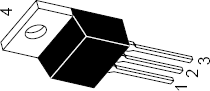 | |
| Relatively Common, (available from Farnel at < $NZ 3) | |
| Has adequate data for approximate model parameter estimation | |
| Appears to have adequate RF performance potential based on Ccb ,FT and Switching Times | |
| Would be a good example to show MicroCap's potential for Linear RFPA Simulation and Analysis |
(I may try a similar design based on the use of a switching MOSFET at a later date)
| Transistor Parameter | Value | Units | Comment |
| Maximum Collector Current IC | 10 | Amps | Continuous, peak ICM = 20 Amps |
| Maximum Collector Voltage VCEO | 80 | Volts | |
| Power Dissipation | 50 | Watts | Case temperature Tc = 25 Celsius |
| DC Current Gain HFE | > 20 (Typical = 150 ) | VCE = 1.0 V, IC = 4.0 Amps | |
| Collector Saturation Voltage | < 1.0 (Typical = 0.23 ) | Volts | IC = 8 Amps, IB = 800 mA |
| Emitter Saturation Voltage | < 1.5 (Typical = 1.0 ) | Volts | IC = 8 Amps, IB = 800 mA |
| Transition Frequency FT | 50 | MHz | VCE = 10 Volts, IC = 500 mA |
| Collector Base Capacitance CCB | 130 | pF | VCB = 10 Volts |
| Collector Emitter Capacitance CEB | - | pF | Not specified |
| Switching Delay and Rise Time Td + Tr | 300 | ns | IC = 5 Amps |
| Switching Storage Time Ts | 500 | ns | IC = 5 Amps, IB1 = IB2 = 500 mA |
| Switching Fall Time Tf | 140 | ns | IC = 5 Amps, IB1 = IB2 = 500 mA |
The D44H11 Power Transistor has a reasonably consistent common emitter current gain ratio HFE across a wide range of collector currents - possibly an indicator of good linearity potential when used in a class AB RF Power Amplifier application. Since the RFPA linearity aspects will be important for SSB and DSB operation, we will make some effort to extract device model parameters that express general non linear characteristics. The first of these characteristics will involve the variation in DC current amplification ratio HFE with device collector current IC .
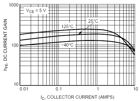
The maximum value for HFE = 180 (approximately, i.e. BF = 180) at IC = 800 mA and falls to ½ this value at IC = 8 Amps (i.e. IKF = 8 in MicroCap device model).
The MicroCap analysis file shows the fall-off behavior in H at high collector currents but not (as yet) at reduced collector currents.
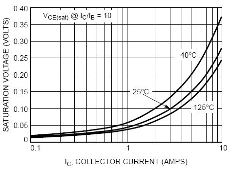
The collector saturation voltage VCE(sat) = 0.02 V @ IC = 100 mA, rising to VCE(sat) = 0.28 V @ IC = 10 Amps. We will interpret this voltage drop to be caused by an equivalent total series resistance Ree + Rcc = [0.28 - 0.02] / [8.0 - 0.1] = 0.026 Ohms .
The collector current versus Base Emitter voltage data is provided but only in device saturation. This is a small complication in parameter estimation but we will use the data to estimate as best we can.
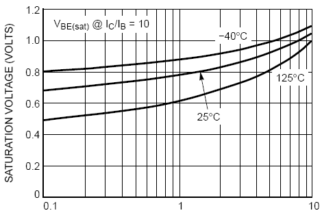
| IC (Amps) | IB (Amps) | VBE (Volts) | Comment |
| 0.1 | 0.01 | 0.68 | T = 25 C estimated from graph |
| 1.0 | 0.1 | 0.78 | T = 25 C estimated from graph |
| 10.0 | 1.0 | 1.04 | T = 25 C estimated from graph |
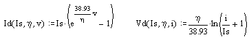
It would be useful to estimate the transistor "saturation current" Is and "Ideality Factor" n from this data. In addition, estimating the parasitic resistances Ree , Rcc and Rbb would be useful. MATHCAD will be used to facilitate this procedure based on the following relationships
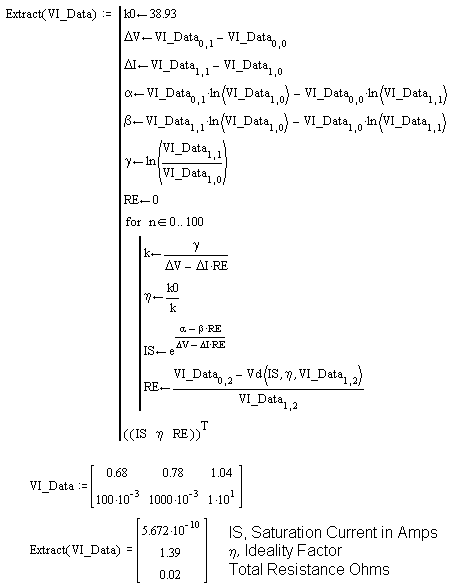
The collector saturation voltage data suggested that Ree + Rcc = 0.026 Ohms, and the MATHCAD algorithm (derived from simultaneous equations using 3 data points) suggests that Ree + Rbb / 10 = 0.02 Ohms. As we found previously in the NPN model, estimating R using this method is prone to error so some guess-work is needed. Fortunately R has a minor effect at medium to low RF frequencies so its accuracy is probably non critical.
We will assume that the collector parasitic resistance will be relatively small and define
Ree = 0.02 Ohms
Rcc = 0.006 Ohms
Rbb = 0.2 Ohms, at medium collector currents for RF behavior.
We note that the device ideality factor n = 1.39 and its saturation current parameter IS = 5.7 · 10-10 Amps in saturation. Since the device was operated with a "forced current gain" equal to 10, the actual saturation current parameter is probably higher (by HFE / 10 if HFE was constant) but we will use the estimate "as is" for this demonstration. (Other devices may include preferable non saturated V-I data)
We observe the same general trend in VBE variation with collector current IC but the actual value of VBE is slightly lower than in the published data presumably due to the lower base current needed for non saturated simulation (compared to published data based on saturated operation)
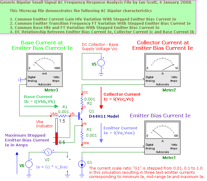
The D44H11 Bipolar transistor will operate in class AB and this will result in its collector current variation from IC = 0 mA up to some maximum peak value. This may require low current HFE behavior to be included in the overall simulation. I have incorporated some parameter estimation based on the following reasoning,
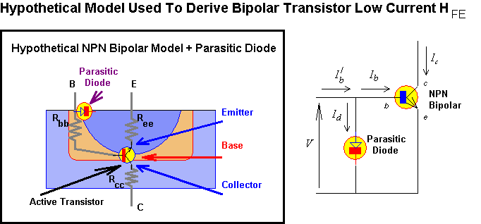
I am proposing this model as a mechanism that can recreate low current H behavior in MicroCap, as opposed to a real mechanism based on actual device physics. The intention is to allow some potential for this non linearity to be included in overall Intermodulation performance in the final simulated RFPA (two tone test).
The :active transistor" is assumed to be buried deep inside the NPN structure where the base thickness is least. A "parasitic diode" (or very low H NPN transistor) is proposed to lay laterally near the surface and "rob" some of the base terminal current from reaching the active transistor site. The collector current Ic of this active transistor is determined by its base-emitter voltage V
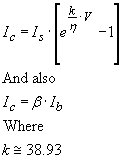 …(1)
…(1)
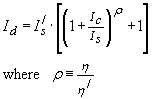
The parasitic diode current will follow a similar relationship but may have different saturation current and ideality factors.
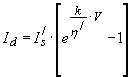 …(2)
…(2)
Note that MicroCap defines
![]()
The base terminal current Ib/ is equal to the sum of the active transistor base current Ib and the parasitic diode current Id . This allows a "composite" current gain (Beta) to be defined as
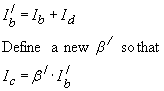 …(3)
…(3)
Now make V the subject in equation (1) and substitute this into equation (2) to obtain
 …(4)
…(4)
Note
![]()
The total base terminal current is then the sum of the parasitic diode and active transistor base currents
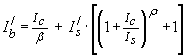 …(5)
…(5)
This results in an overall current gain for the composite diode-transistor pair,
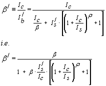 …(6)
…(6)
We now see from equation (6) that the overall current gain is now dependent on collector current Ic . It may be helpful to introduce a reasonable approximation where p ~ 1 and Ic >> Is
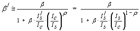 …(7)
…(7)
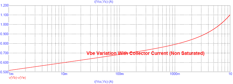
Equation (7) suggests that the relative ideality factor p needs to differ from unity if the current gain has a dependency on collector current. Let us try a MATHCAD simulation now, based on the previous values for HFE , Is and n.
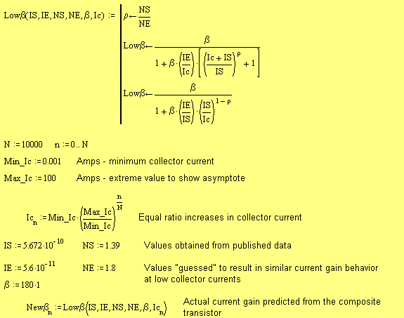
I "juggled" IE and NE to result in similar HFE behavior at low collector currents and let the collector current to run close to its asymptote value for the purpose of demonstration. Also I included a lower collector current range down to Ic = 1 mA compared to published data that was limited to Ic = 10 mA.
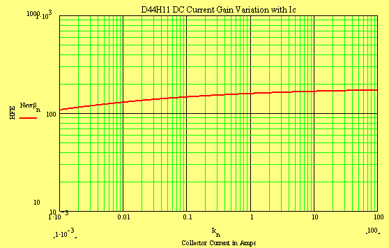
I then updated MicroCap with these device model parameters for the D44H11 transistor

Interestingly, the MicroCap device model is in excellent agreement with my "theory" and the MATHCAD prediction. Perhaps this parasitic diode really does exist?
The DC model parameters appear to be adequately estimated for the D44H11 so now let's estimate some RF relevant parameters. The Forward Transit Time "TF" is related to the Transition Frequency FT as
TF = 1 / [ 2 · pi · FT ] where FT = 50 MHz i.e. TF = 3.2 · 10-9 seconds
The zero bias collector base capacitance "CJC" is related to the published reverse biased junction capacitance as
CJC = CCB{VCB } · [ 1 + VCB / VF ]MJC where VF = 0.75 Volts and MJC = 0.33 as default values
The published collector base capacitance is stated as CCB = 130 pF @ VCB = 10 V implying CJC = 313 · 10-12 F. Unfortunately the base-emitter capacitance data CEB is not listed so we will assume CJE to be slightly larger than CJC i.e. CJE = 500 · 10-12 F with the same value for its "grading coefficient" MJE = MJC = 0.33.
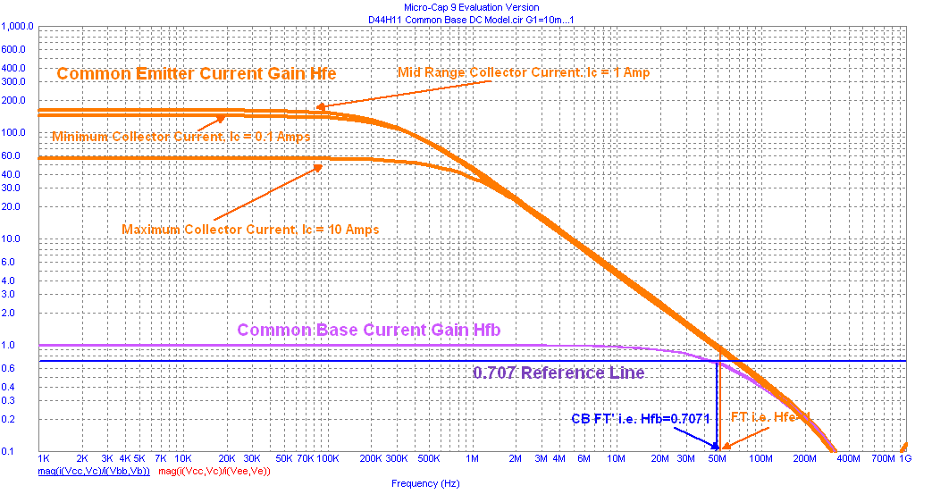
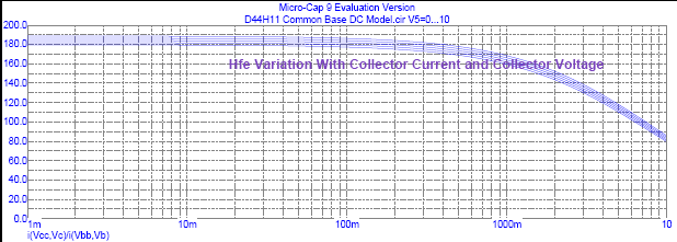
The MicroCap prediction for Hfe variation with frequency and collector current appears to be quite reasonable, with the correct value of FT shown to equal FT = 50 MHz. Although the transistor will operate in "pseudo linear" class AB operation, it will operate as a non saturated switch so it is desirable to include some indication of its switching performance. Admittedly I have not (as yet) achieved great accuracy with the large signal switching model in MicroCap as I suspect that real transistors are quite complicated in this extremely non linear mode of operation. I include the following MicroCap file as an indication for general behavior only.
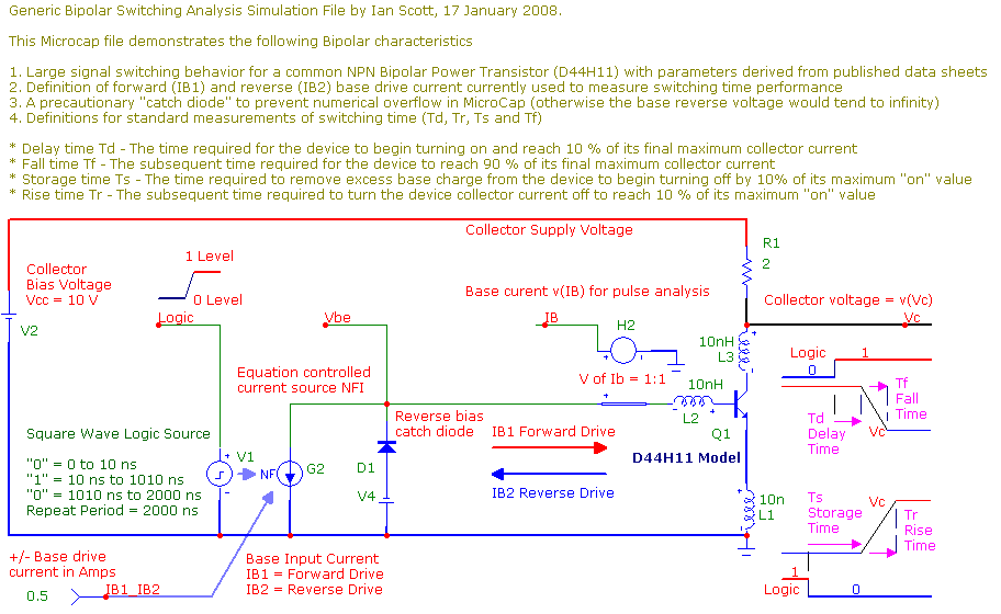
I included extra parasitic lead inductance estimated at 10 nH per terminal and set the device charge storage time to TR = 500 ns. MicroCap produced the following switching response
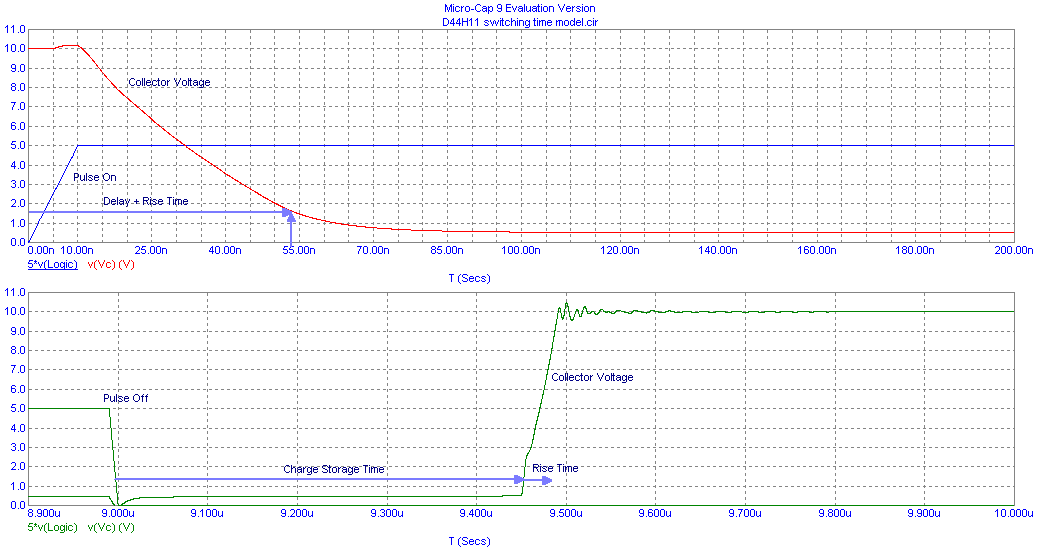
The D44H11 data listed the delay and turn on to be 300 ns, i.e. much longer than the simulated result that is closer to 55 ns. The charge storage time is about 450 ns, close to the listed value of 500 ns, but the simulated rise time appears to be about 50 ns compared to the longer rise time published as 140 ns. Given that these times are very current dependent and that MicroCap's device model may have reduced accuracy at the high collector current range these discrepancies may not be significant TBD!
Level =1
DC Relevant Model Parameters
| BF | IKF | BR | IKR | IS | ISE | ISC | NF | NE | NC | RE | RC | RB | VAF | VAR |
| 180 | 8 | 1 | 0 | 5.672e-10 | 5.6e-11 | 5.6e-11 | 1.39 | 1.8 | 1.8 | 0.02 | 0.006 | 0.2 | 100 | 100 |
AC Relevant Model Parameters
| TF | TR | CJC | MJC | VJC | CJE | MJE | VJE |
| 3.2e-9 | 500n | 313e-12 | 0.33 | 750m | 500e-12 | 0.33 | 750m |
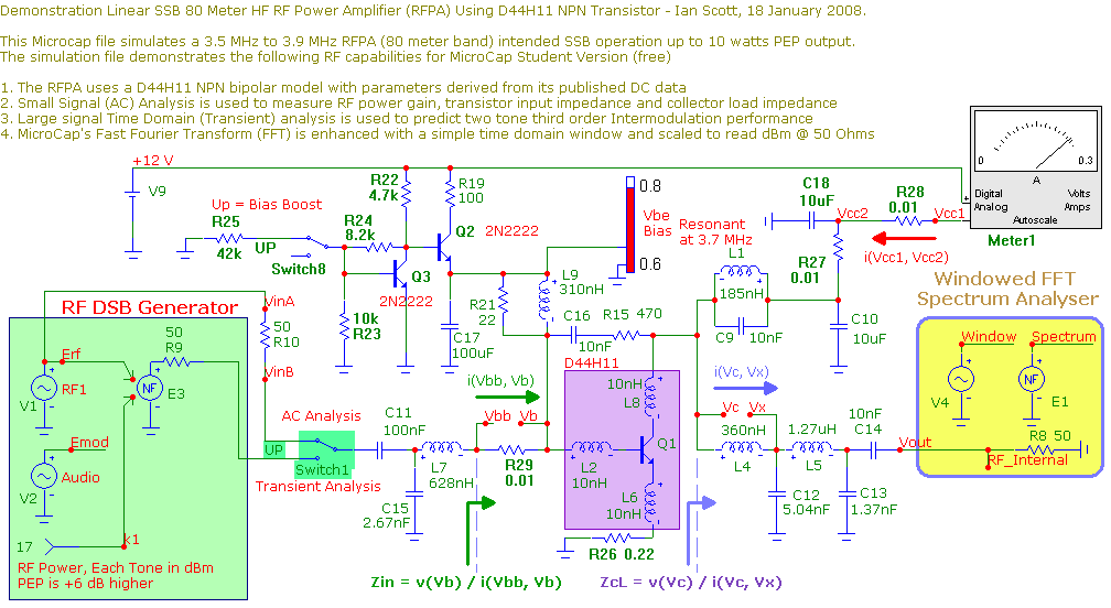
By now we have a proposed device model for the D44H11 NPN Bipolar Power transistor that has been "gleamed" from somewhat meager published data, but hopefully this will be adequate for demonstrating the RF performance of a single ended class AB RFPA intended for HF operation at 3.7 MHz (80 meter frequency band). I plan to build this amplifier later on and see how it goes in practice!
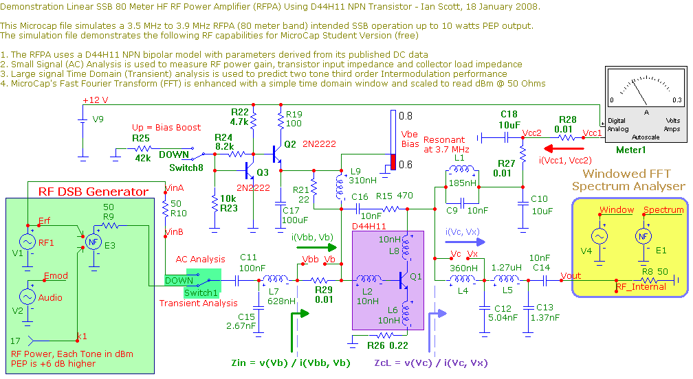
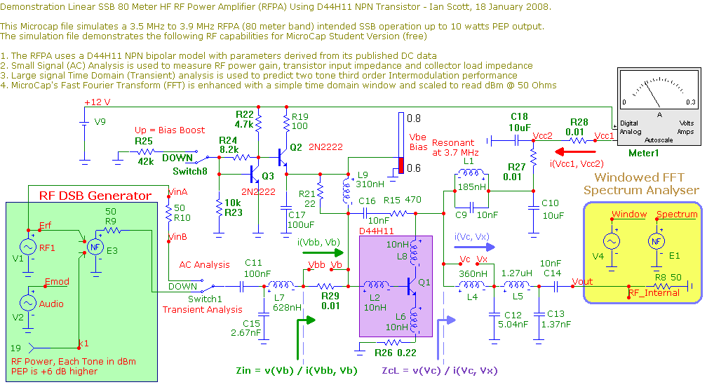
The D44H11 NPN Bipolar power transistor is used in a standard class AB common emitter circuit configuration with lumped element input and output impedance matching networks. This bias voltage to be increased he base bias voltage is provided by Q3 and Q2 and switch8 is included to provide a better indication of small signal RF power gain and input impedance.
Small signal AC analysis is provided when Switch1 is in the "Up" position. The RF power gain (with increased DC bias current) is about 21 dB at f=3.7 MHz and input and output resistance is about 5 Ohms at the transistor terminals. The reactive component for Zin at the base of Q1 is "tuned out" by L9. C15 and L7 transfer this low value of input resistance up to 50 Ohms and L4,C12,L5 and C13 transform the 50 Ohm load impedance down to a collector load impedance of 5 Ohms.
The predicted maximum output power is usually estimated from the following equation
Pout, max = Vs2 / [ 2 · RcL ]
Given Vs = 12 V and RcL = 50 Ohms we predict Pout, max = 14.4 Watts (PEP). This limit should be adequate for the target (linear) output power rating of Pout = 10 Watts PEP.
The base bias "boost" switch has resulted in a collector current of 260 mA (shown on meter1) and the resulting small signal power gain is about 21 dB for the RF power amplifier. This will reduce at normal bias current (about 60 mA) intended for class AB operation, but should still exceed the target large signal power gain of 17 dB.
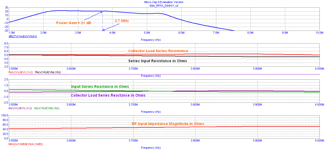
We observe that the RF power gain is relatively constant across the intended RF frequency range of 3.5 MHz to 3.9 MHz but falls off outside this frequency range due to the bandwidth constraints imposed by lumped element input and output impedance matching networks.
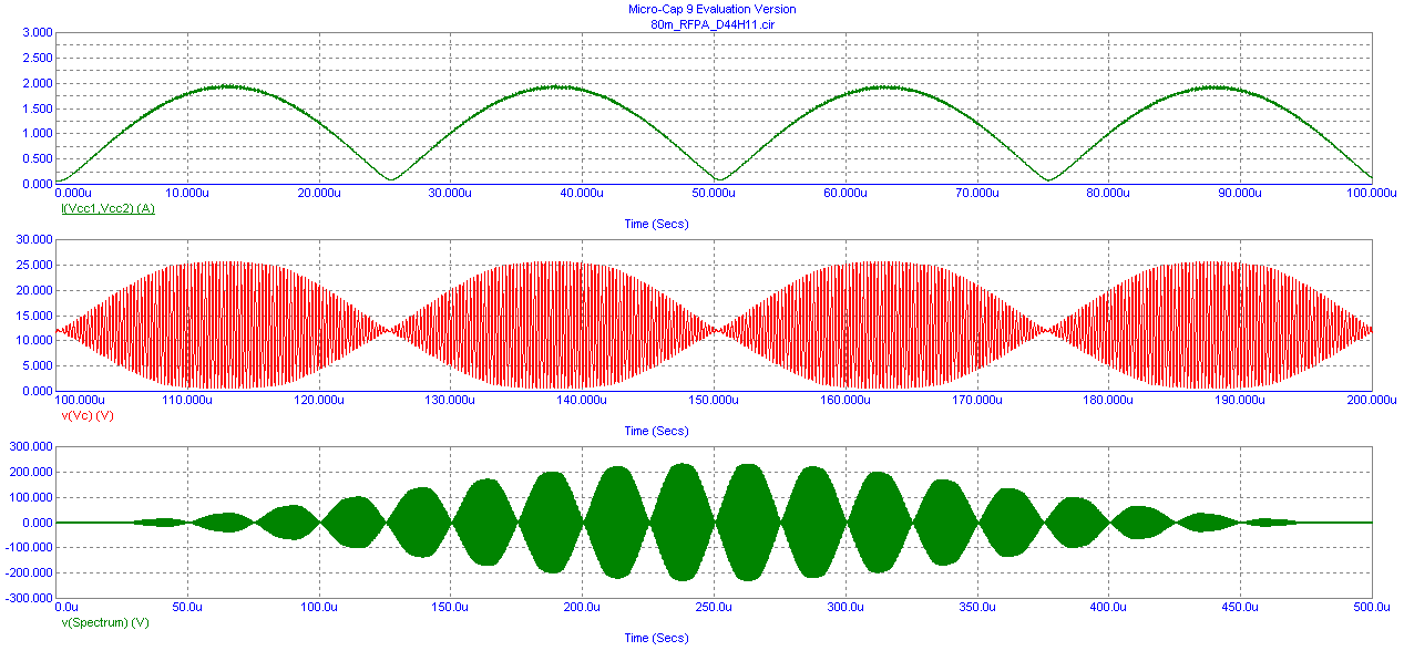
Let's now simulate the large signal behavior of the proposed RF Power Amplifier. I have included a two tone signal source generator with a scaled RF power parameter set to +17 dBm per tone (i.e. +23 dBm PEP RF drive) with a tone spacing of 40 kHz. (i.e. the audio modulating generator has a frequency of 20 kHz). This two tone test signal is presented to the transistor through its input matching network C15, L7 and L9. Some "negative feedback" is included from R15 and R26 as this tends to help suppress instabilities especially at higher than expected RF drive levels. Also I have included a resonant load with L1 and C9 to the transistor collector to reduce the tendency for high collector voltage excursions with Q1 turns off - the high order harmonics are "shorted out" by this network resulting in a near-sinusoidal collector voltage. This precaution is included to assist linearity and improve ruggedness under high load VSWR conditions (if these occur accidentally).
The following simulation shows the time domain variation in collector current, collector bias and the scaled and "windowed" RF output voltage that will be used for FFT spectrum analysis later (the scaling is to present the FFT result in dBm rather than dB_0V - i.e. 10 dB difference).
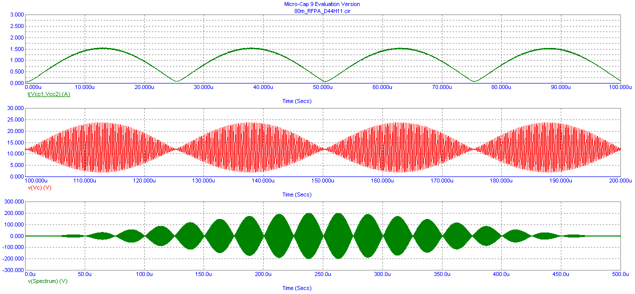
We see the peak supply current is about 1.5 amps i.e. 18 watts DC input power from the supply voltage of Vs = +12 V. The collector voltage variation falls to about Vc = 1 V (i.e. above device saturation) and rises to a maximum value of Vc = +24 V (i.e. an equal variation above the supply voltage showing sinusoidal behavior). The last graph shows the action of the window function (this procedure helps eliminate any degradation in amplitude dynamic range caused by small transient "start up" effects in the RFPA circuit).
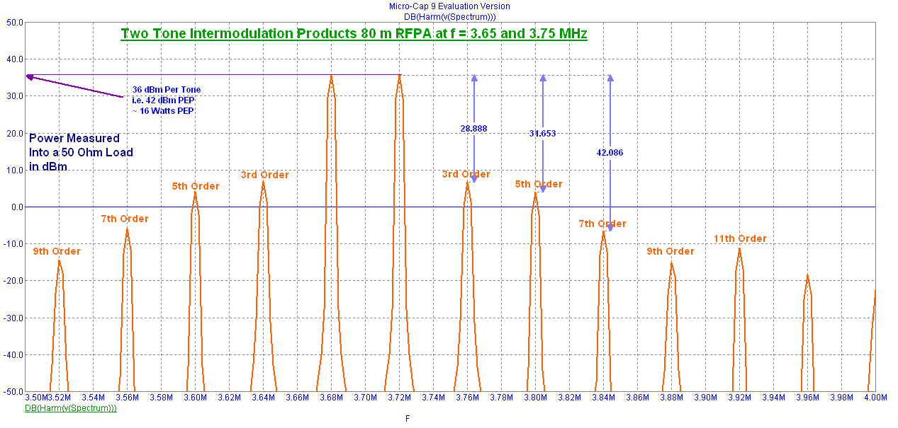
Now let's examine the two-tone output intermodulation performance for the RFPA shown in the following graph.
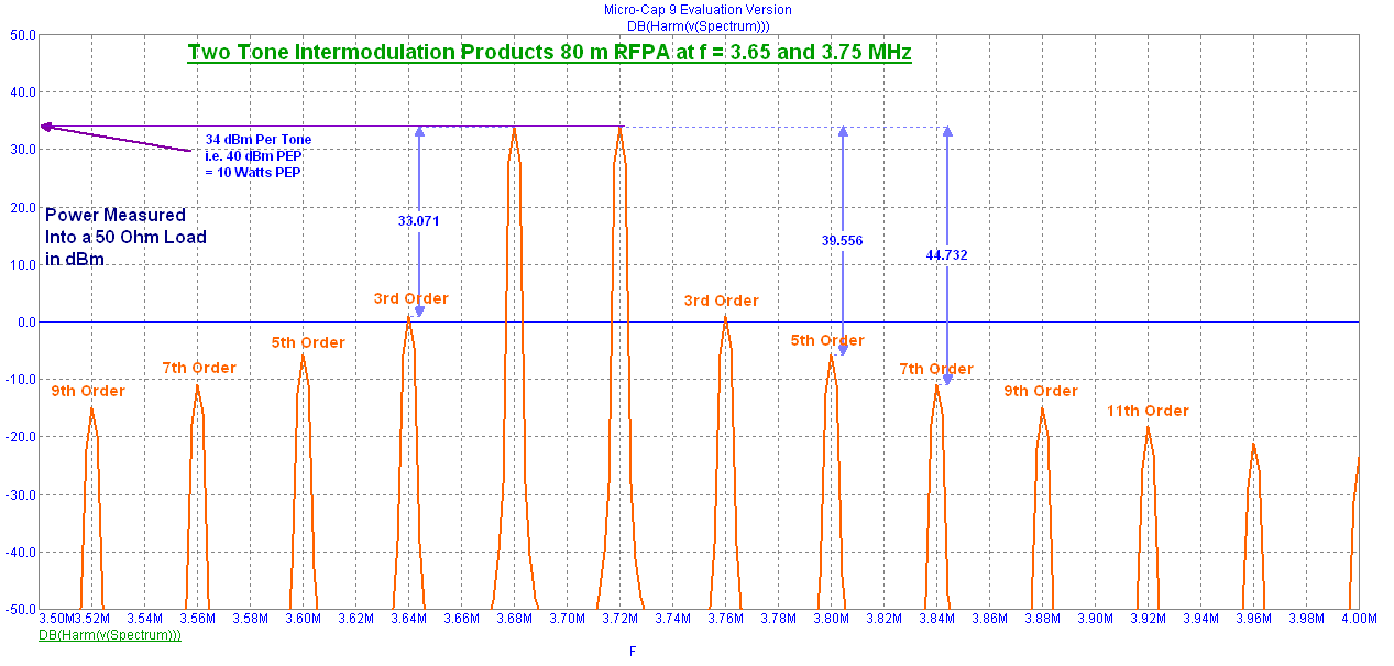
Each RF output tone is about +34 dBm (2.5 Watts) which combine periodically in phase to produce an output voltage that is two times higher, i.e. +6 dB or 4 times in power. This suggests the RF PEP output power achieved is equal to the target design value of Pout = 10 Watts PEP. The third order Intermodulation products appear to be about -33 dB lower than each test tone (which exceeds the design target of -30 dB) and higher order Intermodulation products become progressively smaller. This represents acceptable linear behavior from the RFPA.
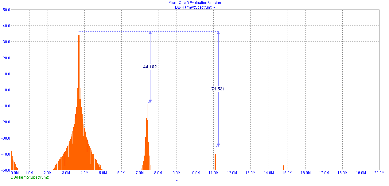
Now let's investigate the harmonic output content under these drive conditions. The following RF Spectrum shows the second harmonic to be ~44 dB lower and the third to be about 71 dB lower. (Note - MicroCap's "scope" features are a bit clumsy and the peak-peak distance measurements don't always land exactly where they were intended!).
Now lets examine the RFPA behavior with +2 dB RF input overdrive, i.e. Pin = +19 dBm per tone.
This time we observe the collector current peak to be about 2.0 Amps, i.e. 24 watts PEP DC input power at Vs = +12 V. We also observe the collector voltage waveform to "bottom out" slightly corresponding to a small amount of device saturation.
The windowed FFT spectral analysis now shows increased RF output power close to 16 Watts PEP but the 3rd and higher Intermodulation products have deteriorated a bit.
Overall summary: The RFPA design appears reasonably well behaved in simulation and could therefore proceed to physical construction and evaluation. The actual RF performance may not be exactly consistent with the simulation (could be better or worse!) but certainly none of the simulation results suggest that using the D44H11 NPN Bipolar power transistor for linear class AB operation at 3.7 MHz would be a bad idea!
I have stretched MicroCap's simulation capability quite a bit in this web chapter but once again, it has come through with some very appealing results. The use of this simulation tool (free student version) certainly allows many aspects of the RFPA circuit behavior to be investigated and this demonstration potential represents a valuable educational tool. The results are somewhat believable, but are based on model parameters that have been estimated from relatively scarce published device data.
The use of any simulation tool should not be considered to result in a "guarantee of outcome" in a final design. It is better, in my opinion, to use simulation tools to "weed out" the obviously unsuitable approaches and to demonstrate some insights into general circuit trends and waveforms. Simulation results can therefore highlight certain areas to look into in more detail (e.g. instability at high RF overdrive, temperature and component sensitivity, etc) and indicate potential outcomes. Given the high expense and typical shortage of RF test equipment in many development labs and home hobbyist workshops, preliminary simulation effort is well spent.
I have used MicroCap in these web chapters because it can be downloaded as a free student version from Spectrum Software at
http://www.spectrum-soft.com/index.shtm
and has unlimited usage time but some restrictions on device model availability and maximum component count. No doubt many other "Spice based" circuit simulators are available (Electronic Work Bench http://www.ni.com/academic/multisim.htm etc?) and each may have individual features of interest.
I hope this web chapter has helped to illustrate some of the principles of linear RF Power Amplifier design based on a planned amateur radio project I am considering. I plan to build this circuit later in the year along with other circuits listed here (e.g. 80m RF VCO) and I hope to publish the outcomes when they are available.
I guess the burning question is "will they actually work in practice" ! ?)
![]()
Return to Microcap Simulation
or Ian Scotts Technology Pages
© Ian R Scott 2007 - 2008