or return to Kaleidoscope Comms
The intention here is to demonstrate a design methodology that can be applied to medium power HBT RF Amplifier development at medium frequencies, e.g. 433 MHz. Although many IC solutions exist in a similar output class, and can have extremely low component count, these are typically limited to 800 MHz and above, and their use of internal impedance matching may prevent operation down to 433 MHz etc. 1 Watt amplifiers such as Sirenza SPA-2118 and Skyworks CX65104 both provide >30 dB of gain at 800 MHz, but are not well suited for operation at 433 MHz due to internal matching. (More extensive in the Skyworks part but the Sirenza version has at least one internal matching network on the base of its output HBT.
Some IC's are available that include operation down to 400 MHz, e.g. MAX2430 but these have limited output power e.g. 21 dBm or 125 mW.
Wideband MMIC amplifiers are popular, based on a negative feedback darlington configuration and operate from DC to 6 GHz so with minor gain variation. These are usually limited to 50 mW or 17 dBm output power, but some possibility exists for slightly higher power versions to become available. The difficulty is that wide band operation assumes the absence of any output matching network so the device will have to operate into 50 Ohms directly. In order to achieve 1 Watt into 50 Ohms, you need 7V RMS of voltage, or 12 Vpeak. Unfortunately the high FT HBT technology needed for wideband tends to have much lower breakdown voltages than this. The use of SiC (Silicon Carbide Semiconductor) may modify this limitation in future, but current SiC devices have fairly low frequency capability and are really only available commercially as high power Schottky diode rectifiers.
It appears therefore an IC solution will either be power limited or frequency limited. A module solution may be available though, but possibly at the other power extreme, e.g. 7 Watts or higher.
It appears sensible therefore to consider a discrete solution, at least for the final output stage.
There are two most suitable candidates,
LDMOS : e.g. PD55003 from ST or consider NEC etc
Standard BJT : BFG235 500 mW from Infineon
SiGe HBT : MAX2602 1 Watt HBT from Maxim or
SiGe HBT : SGA9289 800 mW HBT from Sirenza.
LDMOS is well suited power output power levels above 3 Watts and can work at 3 V supplies up to 28 V depending on the device. They require gate bias set-up which suggests a manual adjustment or the use of a DAC control device. However class A operation is possible, and a 3 Watt PD55003 could be used at 1 Watt output as class A, and when overdriven, will slide towards class AB.
The BJT and HBT alternative may however be simpler in some regards, and will generally have less difficulty with RF stability, depending on the design of associated matching networks.
The BFG235 is an older generation standard Bipolar transistor with a low FT about 5.5 GHz but has a collector dissipation of 2 Watts, and may be capable of outputs up to 1 Watt, but 500 mW may be more practical. It will have relatively low gain, 10~12 dB at 433 MHz and requires a supply voltage between 8 V and 10 V to achieve this. S-parameter information may be absent.
The MAX2602 1 watt HBT is also suitable, but also lacks s-parameter information and has scant, and perhaps dubious large signal impedance data. The SGA9289 in comparison has s parameter data and application notes. It also has much higher gain than the MAX2602, approximately 10 dB.
For the purpose of a tutorial, it is necessary to start with well characterized devices so that the design methodology can be demonstrated. The SGA9289 HBT from Sirenza will therefore be selected.
|
Parameter |
Target Value |
Units |
Comment |
|
Supply Voltage |
5.0 |
Volts |
Maximum device recommended value |
|
Supply Current |
270 |
mA |
S Parameter data provided at this bias point |
|
Center Frequency |
433 |
MHz |
|
|
Bandwidth |
20 |
MHz |
|
|
Power Gain |
20 |
dB |
Minimum |
|
Output Power |
19 |
dBm |
At 1~2 dB gain compression |
|
Harmonics |
-10 |
dB |
A post amplifier Low Pass Filter is expected |
|
Input Return Loss |
10 |
dB |
Over operating bandwidth |
The HBT will be biased for class A operation and use active bias to prevent changes in bias current as RF is applied. This effective mode will slide into class AB as RF input drive is increased, as base emitter rectification will cause the device Vbe to reduce.
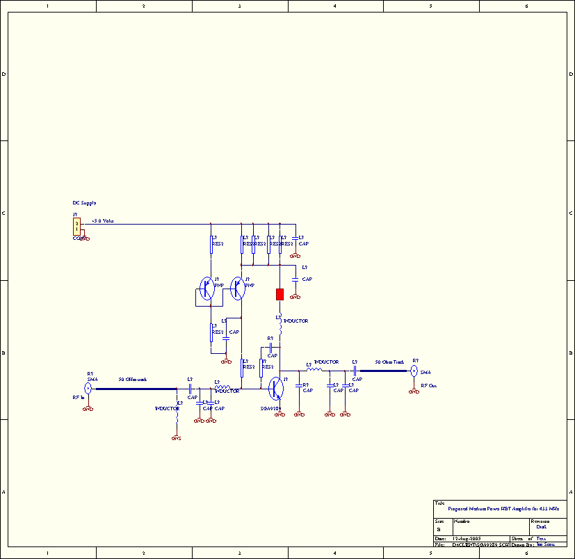
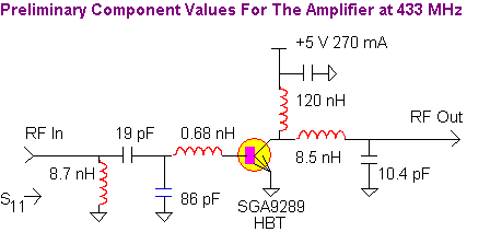
A single SGA9289 HBT is used as the amplifying device with a N=4 High Pass- Low Pass input match and N=2 Low Pass output match. Collector Base resistive feedback is used to enhance stability and reduce gain which otherwise could be excessive. DC bias is applied to the collector through an inductor with a series ferrite bead, intended to enhance stability under some VSWR conditions. A dual audio PNP transistor is used for active bias and ensures a near constant collector current despite changes in RF input drive level and output load conditions.
The SGA9289 HBT will be biased at 270 mA collector current and a collector voltage of 4.7 V, as 300 mV will be allocated to the active bias circuit. This corresponds to a DC power input of 1.27 Watts, which would correspond to an output power of 630 mW at a conversion efficiency of 50 % and 761 mW at 60 % efficiency. The final efficiency depends on the extent of RF input overdrive, but an output power of 700 mW does not seem unreasonable. Some increase in the collector bias current may allow the target 800 mW to be met, on average. This will require some final component value adjustment, but the 800 mW target does not seem impossible.
The optimum collector load will be approximately
![]() ...(equation 1)
...(equation 1)
where // means
where // -Cout is defined as "in parallel with an inductance corresponding to the output capacitance Cout of the device"
This predicts RL ~ 17.4 Ohms. The device output capacitance Cout can be approximately estimated from the published output load impedance of the SGA9289 HBT under similar bias conditions. Unfortunately this is not listed at 433 MHz, but will be assumed to be relatively constant for the purpose of this tutorial.
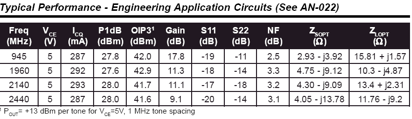
Let us consider the 945 MHz data. At Vce = 5 V, Ic = 287 mA, then we would predict RL = 17.4 Ohms. We note that ZLopt = 15.8 Ohms + j 1.6 Ohms, which we can convert to parallel form using the following series to parallel impedance conversion formula
![]() ...(equation 2)
...(equation 2)
These equations are fundamental to reactive impedance matching and should be committed to memory. From the published data we find that Rp = 16.0 Ohms and Xp = 158 Ohms, at 945 MHz. Since
![]() ...(equation 3)
...(equation 3)
we predict that Cout = 1.1 pF. We note that the predicted optimum load was 17.4 Ohms, which closely matches this published derivation of 16.0 Ohms, presumably due to a small device saturation voltage. However we can consider both loads to be within variation caused by component tolerances, measurement uncertainty or the exact target performance under evaluation, which in this published data might be a linearity criteria given the two tone stimulus used.
We will elect to remove the parallel capacitance term Cout by resonating this with the collector inductance, although it can equally be removed with a series inductance given that the output load is converted back to series impedance term. The value of collector supply inductance is given by
![]() ...(equation
4)
...(equation
4)
Using the above values we find that a value of Lp = 120 nH at f = 433 MHz.
We want to now determine the output matching components for the N=2 reactive match topology. Equation 2 can be used for this, since we know Rs ~ 17.4 Ohms, approximately and the final Rp = 50 Ohms
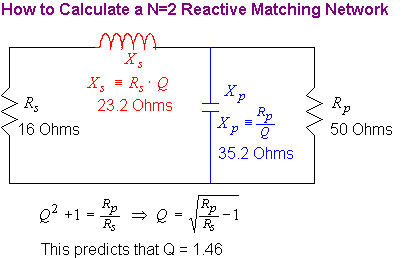
Equation 3 and Equation 4 now let use determine the inductance and capacitance values at f = 433 MHz, i.e. Ls = 8.5 nH and Cp = 10.4 pF.
These are ideal values, and some allowance will need to be made for PCB and component strays, or to adjust the final values to suit available component values. For example, lets say the only available inductances values are 6.8 nH or 10 nH. If we select the 6.8 nH component then we will need to add an extra 1.7 nH of track inductance, generally directly from the collector terminal of the HBT device. The inductance of PCB track is the same as that for transmission line, and providing you know the PCB track impedance Z0 and its velocity factor vf then this can be readily estimated from
![]() ...equation 5.
...equation 5.
If standard FR4 PCB material is used, the relative permitivity
![]() will
be about 4.8. It is often convenient to choose PCB dimensions so that the
characteristic impedance Z0 = 50 Ohms, unless special considerations
suggest otherwise. From equation 8 we would predict the additional collector
track length, corresponding to 1.7 nH to be 4.7 mm.
will
be about 4.8. It is often convenient to choose PCB dimensions so that the
characteristic impedance Z0 = 50 Ohms, unless special considerations
suggest otherwise. From equation 8 we would predict the additional collector
track length, corresponding to 1.7 nH to be 4.7 mm.
The effective Z0 of PCB track can be estimated from
 ...(6)
In this case h represents the substrate height and w represents the width of the track. Using MATHCAD we can make some general predictions, in this case for a substrate height of 0.3 mm based on FR4 material
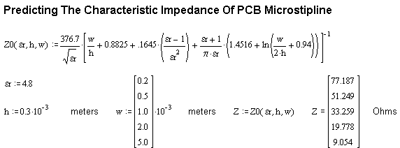
In these examples, 50 Ohm track corresponds to a microstripline track width of about 0.5 mm.
An alternative is to add a capacitor in series with the inductor to "tune out" excess inductance. Let us assume a 10 nH inductor was selected and we only required 8.5 nH, i.e. we have an excess inductance of 1.5 nH. From equation 4. we would predict an equivalent series capacitance of Cs = 90 pF at f = 433 MHz.
A final consideration is the actual lead inductance of the capacitors used, as this will cause their "effective capacitance" to increase with frequency, so a smaller value than predicted would be used to compensate. This lead inductance depends on the capacitor size and PCB geometry, and may vary from 0.3 nH to 3 nH quite easily. As the PCB material thickness is reduced, this lead inductance also decreases, but not proportionally. Also smaller components such as 0402 SMD will have less inductance than larger 0805 types.
From the published large signal data we see that Zsopt = 2.93 - j 3.92 Ohms at f = 945 MHz. This appears suspicious as the negative j sign suggests a capacitive source reactance is best, but then for what performance target parameter? Does this source impedance value correspond to maximum power gain, lowest Noise Figure, best Intermodulation distortion or some in-between combination of all three? What appears likely though is that the source impedance is very low. A N=2 input match might therefore be narrow band, so perhaps a N=4 input match would be better. This would allow similar bandwidth performance between input and output.
If we look at the S-Parameter file we see a slightly different story.
| F, MHz | Mag S11
dB |
Ang S11
Degrees |
Mag S21
dB |
Ang S21
Degrees |
Mag S12
dB |
Ang S12
Degrees |
Mag S22
dB |
Ang S22
Degrees |
| 400 | -.5853 | 177.02 | 16.662 | 85.139 | -37.741 | 38.908 | -2.2428 | -177.44 |
| 450 | -.5681 | 176.07 | 15.628 | 83.79 | -37.832 | 36.344 | -2.2114 | -178.58 |
If we first concentrate on S11, we can convert this to impedance using the following
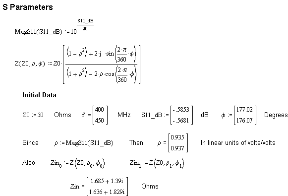
Quite often S Parameters are given in linear units, which is easier. However we see that the input impedance is low, and inductive, which is consistent with the need to have a conjugate source impedance, i.e. capacitive. However this information is at least now available at 433 MHz, approximately in-between the two frequency points given at 400 and 450 MHz. However this represents the impedance when the output of the HBT device is terminated in 50 Ohms, what would it be when the termination is 17.4 Ohms in parallel with -1.1 pF, as we saw a while back?
It is possible to determine the new input impedance, directly from S Parameters. The equation is
![]() ...equation
7.
...equation
7.
However the parameters need to be presented in x + j y format. Consequently this is not a procedure to carry out on paper, and it is best to allow a simulation tool to fine tune the design. Further, the final design may have excessive power gain and be unstable with optimum matching. In this case some degree of resistive loading or negative feedback will be needed. This complicates direct recalculation of S11.
A suggested methodology is to just start with Zin predicted from S11 with a 50 Ohm collector termination, at least as a starting point. A matching network can then be designed to transform this impedance up to 50 Ohms, if this is the target source resistance. Then the output match can be added to the HBT device, based on its published S-Parameter file, and a linear circuit simulation tool such as ADS, Eagleware or TOUCHSTONE can be used to demonstrate the degradation in input return loss caused by a non 50 Ohm collector termination. If this appears adequate, then the design may be complete. If the input return loss degradation is excessive, then the input matching values can be "optimized", keeping the output matching constant. This is the procedure this tutorial will adopt.
Even so, it may occur that instability is observed, which will show up as S11 or S22 magnitudes exceeding 0 dB at the amplifier input or output. If so, then resistive loading is required, usually in parallel with the base, or in series with the gate for LDMOS devices. Further stability is achieved with resistive feedback from collector to base. These measures will reduce amplifier gain, but often only by a minor amount.
The device power gain with 50 Ohm source and load impedances will be
![]() ...equation
8.
...equation
8.
presented in linear V/V terms. In the published data previously shown, at 15.628 dB directly. The final amplifier gain will be higher of course, as power is lost due to impedance mismatch between device input and output terminations. This mismatch loss is recovered through input and output impedance matching networks.
The power gain lost through mismatch is
![]() ...equation
9.
...equation
9.
Sxx can be either S11 or S22 in linear V/V terms, or if it's expressed in dB as Sxx, dB then the conversion is equally straightforward. For example, if S11, dB is given as -6 dB, then |S11| = 0.5, and if the input match is added, then 1.26 dB of lost gain will be recovered. The same effect will occur with the output match but not simultaneously. However predicting both losses provides a useful indication of achievable gain for initial device selection. (A simulation tool with take account of interactions and provide an exact estimation, but will take much longer to set up and run).
Using the published SGA9289 data as an example we predict
|
f MHz |
S21 dB |
S11 dB |
Lost Gain in S11 dB |
S22 dB |
Lost Gain in S22 dB |
Maximum Gain dB |
|
400 |
16.6 |
-0.58 |
9.0 |
-2.2 |
4.0 |
29.6 |
|
450 |
15.6 |
-0.56 |
9.2 |
-2.2 |
4.0 |
28.8 |
If the input alone is matched, the new amplifier gain will 15.6 + 9.0 = 24.6 dB at 450 MHz. If the output alone is matched, the new amplifier gain will be 15.6 + 4.0 = 19.6 dB. Although these increases do not add independently simultaneously (unless the transistor is unilateral, i.e. no internal feedback), they give a quick indication of what may be achievable in a practical, stable design. The HBT transistor is likely to become unstable if both input and output impedances are matched, or the final matching accuracy will be poor in both directions. This is because the impedances presented by the transistor are interactive with the matching networks. Still, the estimate is simple and provides a quick indication of the gain capability of the transistor. Certainly, the gain target of 20 dB is well within the SGA9289's capability, and even 25 dB may well be feasible with adequate stability.
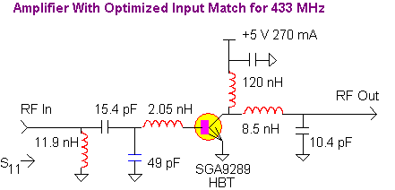
So far it appears that the SGA9289 will be a suitable candidate for the target specification. However we recall that the input impedance, based on S Parameters was somewhat low, that is 1.636 + j 1.826 ohms at 450 MHz. We will therefore transform in impedance in two steps, first from 1.636 Ohms to an intermediary value, and then from this to 50 Ohms.
A good initial approach is select the geometric value between the two resistive term, e.g.
![]() ...equation
10.
...equation
10.
In this case Ri = 9.0 Ohms. We can now draw the impedance matching strategy (shown in reverse order in analogy with the output match)
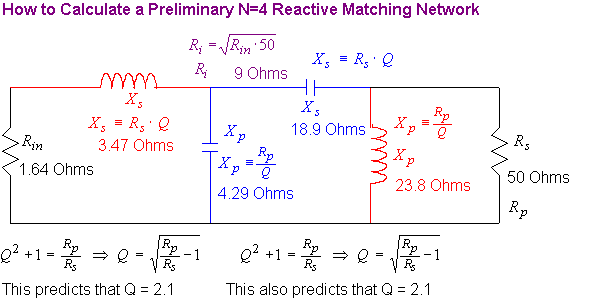
Since the device input impedance already has 1.89 ohms of reactance in series, we will subtract this from the initial value of 3.47 Ohms to arrive at 1.84 Ohms of inductive reactance required in series with the base of the HBT.
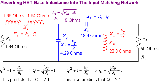
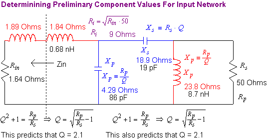
Based on an operating frequency of 433 MHz we can now convert to inductance and capacitance as before. The resulting topology then becomes
So far we have followed a design procedure that allows the output network to be synthesized with reasonable accuracy based on large signal considerations. Then we used the S Parameter data to synthesize an input matching network, which was based on an unmatched output termination. This will result in some inaccuracy, but the extent of this can be simulated. The expected power gain was also estimated, based on the device power gain in a 50 Ohm system, and the added gain that would occur if input and output mismatch losses were removed.
The following simulation result shows input match accuracy, forward power gain, reverse power gain, output match accuracy, and two estimates for unconditional stability, "K" and "B1" across a range of frequencies. We notice the input match is relatively poor, only -7.6 dB at f = 440 MHz, which resulted from the modified output load presented to the collector of the device, as opposed to 50 Ohms where the S Parameters were obtained. The forward power gain is 25.4 dB, not far below the previous approximate estimate of 28.8 dB, at a slightly higher frequency of f = 450 MHz. The output match accuracy is worse again, but remember the impedance presented to the HBT transistor was intended for a large signal power match, rather than best small signal impedance match, so the result is expected.
The last two parameters are indications of unconditional stability. For this to occur, K should be greater than 1 and B1 should be greater than 0. Unconditional stability allows any source and load impedance to be presented to the amplifier without self oscillation. In a power amplifier circuit, the output load impedance is uncontrolled but the source impedance can be fixed, especially is a wide band 50 Ohm MMIC driver is used. Unconditional stability is therefore not essential in power amplifiers, unless the complete line-up is considered.
FREQ-MHZ  DB[S11]  DB[S21]  DB[S12]  DB[S22]        K       B1
           RF_AMP   RF_AMP   RF_AMP   RF_AMP   RF_AMP   RF_AMP

 300.000   -1.257   21.929  -36.332   -8.818    0.639    1.494
 320.000   -2.042   23.369  -34.447   -6.656    0.672    1.193
 340.000   -3.211   24.512  -32.827   -5.278    0.706    0.865
 360.000   -4.648   25.170  -31.371   -4.295    0.726    0.545
 380.000   -6.001   25.370  -30.095   -3.729    0.732    0.302
 400.000   -7.017   25.307  -29.096   -3.674    0.741    0.184
 420.000   -7.641   25.408  -28.632   -3.941    0.742    0.169
 440.000   -7.595   25.384  -28.274   -4.172    0.744    0.167
 460.000   -7.156   25.208  -28.007   -4.313    0.763    0.154
 480.000   -6.656   24.907  -27.808   -4.310    0.797    0.117
 500.000   -6.333   24.608  -27.592   -4.130    0.833    0.046
 520.000   -6.022   24.449  -27.276   -3.619    0.852   -0.101
 540.000   -6.021   24.362  -26.880   -3.101    0.872   -0.285
 560.000   -6.483   24.386  -26.310   -2.513    0.886   -0.542
 580.000   -7.545   24.500  -25.596   -1.847    0.897   -0.888
 600.000   -8.347   24.442  -25.051   -1.253    0.908   -1.191
We note that K is slightly less than desired, and B1 is as low as -1.191 at 600 MHz. Bear in mind that stability is required on any frequency, not just the signal frequency applied to the amplifier.
The simulation tool was then used to adjust the input matching values based on improving input return loss.
FREQ-MHZ  DB[S11]  DB[S21]  DB[S12]  DB[S22]        K       B1
           RF_AMP   RF_AMP   RF_AMP   RF_AMP   RF_AMP   RF_AMP
 300.000   -3.321   25.207  -33.054   -8.633    0.639    1.209
 320.000   -5.705   26.268  -31.549   -6.093    0.672    0.777
 340.000   -9.309   26.789  -30.550   -4.774    0.706    0.418
 360.000  -13.925   26.814  -29.727   -4.102    0.726    0.184
 380.000  -18.565   26.565  -28.900   -3.803    0.732    0.047
 400.000  -22.446   26.245  -28.158   -3.829    0.741   -0.017
 420.000  -24.701   26.214  -27.826   -3.975    0.742   -0.034
 440.000  -23.987   26.197  -27.461   -4.090    0.744   -0.067
 460.000  -24.685   26.122  -27.093   -4.256    0.763   -0.115
 480.000  -25.175   25.950  -26.765   -4.489    0.797   -0.164
 500.000  -19.178   25.705  -26.495   -4.679    0.833   -0.201
 520.000  -14.256   25.532  -26.193   -4.619    0.852   -0.270
 540.000  -10.102   25.164  -26.077   -4.540    0.872   -0.273
 560.000   -6.711   24.450  -26.246   -4.212    0.886   -0.200
 580.000   -4.150   23.232  -26.864   -3.594    0.897   -0.055
 600.000   -2.463   21.492  -28.001   -2.957    0.908    0.130
We note the input match has improved to from -7.6 dB to -24.6 dB, and the forward power gain from 25.4 dB
to 26.2 dB. The K values have stayed the same, but negative B1 values occur over a much wider frequency range.
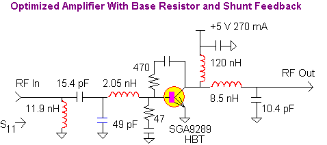
The new circuit values are now
A base resistance of 47 Ohms was added from base to AC ground, (DC blocked with a series capacitor). Also a 470 Ohm resistor was added from collector to base, in a similar manner. The new amplifier S Parameters became
FREQ-MHZ  DB[S11]  DB[S21]  DB[S12]  DB[S22]        K       B1
           RF_AMP   RF_AMP   RF_AMP   RF_AMP   RF_AMP   RF_AMP
 300.000   -4.704   25.602  -31.238  -12.496    0.884    0.963
 320.000   -8.458   26.554  -29.958   -9.100    0.886    0.556
 340.000  -14.818   26.885  -29.256   -7.411    0.889    0.284
 360.000  -27.751   26.720  -28.720   -6.540    0.885    0.151
 380.000  -29.510   26.325  -28.133   -6.111    0.874    0.090
 400.000  -23.507   25.915  -27.567   -6.046    0.866    0.070
 420.000  -20.192   25.851  -27.314   -6.162    0.855    0.071
 440.000  -18.321   25.819  -27.010   -6.209    0.844    0.050
 460.000  -17.306   25.726  -26.693   -6.306    0.846    0.018
 480.000  -16.080   25.524  -26.417   -6.509    0.863   -0.004
 500.000  -13.518   25.242  -26.201   -6.741    0.881 -6.1e-04
 520.000  -10.833   24.996  -25.999   -6.830    0.889    0.001
 540.000   -8.047   24.554  -25.983   -6.952    0.897    0.074
 560.000   -5.507   23.790  -26.219   -6.617    0.902    0.200
 580.000   -3.463   22.575  -26.845   -5.609    0.905    0.343
 600.000   -2.058   20.884  -27.944   -4.433    0.909    0.472
Adding a 3 dB attenuation in front of the previous amplifier immediately improves the stability at the expense of 3 dB gain
FREQ-MHZ  DB[S11]  DB[S21]  DB[S12]  DB[S22]        K       B1
           RF_AMP   RF_AMP   RF_AMP   RF_AMP   RF_AMP   RF_AMP
 300.000  -11.139   22.429  -34.411  -12.616    1.874    0.947
 320.000  -15.065   23.380  -33.132   -9.195    1.471    0.802
 340.000  -21.895   23.718  -32.423   -7.472    1.291    0.694
 360.000  -38.436   23.562  -31.879   -6.560    1.207    0.632
 380.000  -32.552   23.172  -31.287   -6.088    1.156    0.599
 400.000  -28.151   22.763  -30.719   -5.984    1.131    0.591
 420.000  -25.392   22.701  -30.464   -6.069    1.113    0.595
 440.000  -23.881   22.668  -30.160   -6.093    1.086    0.591
 460.000  -23.283   22.573  -29.846   -6.180    1.075    0.588
 480.000  -22.602   22.366  -29.575   -6.389    1.089    0.591
 500.000  -20.328   22.076  -29.367   -6.638    1.118    0.601
 520.000  -17.636   21.823  -29.173   -6.751    1.133    0.605
 540.000  -14.752   21.371  -29.165   -6.894    1.183    0.626
 560.000  -12.112   20.600  -29.409   -6.578    1.264    0.643
 580.000   -9.986   19.382  -30.038   -5.588    1.389    0.633
 600.000   -8.513   17.696  -31.133   -4.424    1.597    0.598
Now k is greater than 1 at all frequencies and B1 is positive. This suggests the combination is now unconditionally stable. The forward power gain of 22.7 dB still exceeds the initial target gain of 20 dB.
For inductor values less than a few nH, printing on PCB is recommended. Equations 5 and 6 provide the means for this transformation.
This Medium Power RF Amplifier tutorial has shown a methodology based on the use of a SGA9289 HBT from Sirenza. Preliminary component values are determined in a pragmatic way, followed by some fine tuning on a linear simulation tool. The gain improvement was only about 1 dB following this fine tuning.
Stability however degraded after this optimization, applied to the input match, holding the output values constant. Base loading and negative feedback showed a small improvement in stability with about an equal loss of gain. Unconditional stability was achieved however, simply by placing a 3 dB attenuation pad in front of the amplifier. Even then, over 2 dB gain was available over then 20 dB target.
If you want to see another design example on microwave class A GASFET amplifier design based on a MATHCAD file, or a class A bipolar amplifier with resistive series-shunt negative feedback why not visit
Return to main page Kaleidoscope Comms