![]()
MicroCap student version comes with a somewhat limited selection of bipolar transistor models such as 2N2905, 2N2222, 2N2369, 2N3055 and quite a few (less common in the west) 2SCxxxx types. It does allow you to create new models but the "model extraction" component is disabled. New device models can still be made manually however.
This MicroCap file will use the NPN 2N2369 bipolar to illustrate a manual extraction method. This is not accurate, however the 2N2369 model has an obvious inaccuracy itself despite have been generated from this extraction component! This will be demonstrated.
The actual transistor model parameters are "silicon fabrication" based and do not directly relate to electrical parameters such as HFE , FT , RBB etc. It is necessary to therefore "infer" these physical parameters from published electrical data using a generic transistor test circuit file.
I have arranged this circuit topology to allow control of the base current I_base and report this base current back as IB_DC. It is important to note that MicroCap displays node voltages or currents are relationships between these (e.g. Vout / Vin would be voltage gain if Vout and Vin are applied as node labels).
The circuit file uses ideal "current to voltage" (V of I) converters and an ideal "voltage to current" (I of V) converter to monitor or inject test signals. The node Ic monitors collector current and presents it as a voltage with a 1:1 ratio. The node Vbe monitors base voltage. The node IB_AC allows a current to be injected into the base through a "I of V" converter to allow current gain to be measured as a voltage ratio HFE = v(Ic) / v(IB_AC).
This may seem convoluted but it demonstrates how flexible the simulation software environment can be. Ideal converter do not exist in the real world but do in a simulation tool. These are not part of a real circuit but allow a real circuit to be inspected without disrupting its operation.
Note: HFE and Hfe are defined differently as DC and AC current gain parameters - this model analyzes both so I use them interchangeably in text description of the analysis circuit design.
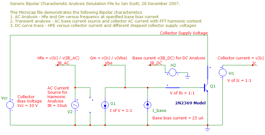
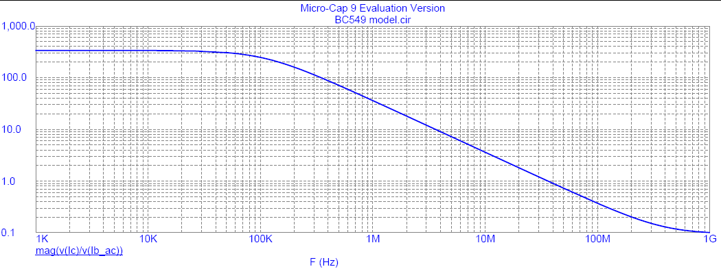
The AC Analysis option is used to display Hfe = v(Ic) / v(IB_AC) with frequency from 1 kHz to 1 GHz with a base bias current of 25 uA. The y axis is selected to be a Logarithmic scale and shows a low frequency current gain of about 80, implying a collector current of 80 * 25 µA = 2.0 mA. We notice that Hfe = 1 at F = 280 MHz, therefore FT = 280 MHz. The -3 dB falloff point will be FT / Hfe = 3.5 MHz which also agrees reasonably with the first graph. The "physical silicon model parameter" in MicroCap is "forward transit time" TF = 221.442878p (pico seconds) - this should be a scaled version of the transition frequency FT but by what ratio? Now the term "pi" is often included in this scaling, not that 1 / [ 4 · pi · FT ] = 280 p. Therefore if we want to model a new transistor with a different FT then it seems reasonable to use the same relationship, especially given that many bipolar transistors have device to device spreads of FT greater than two to one!
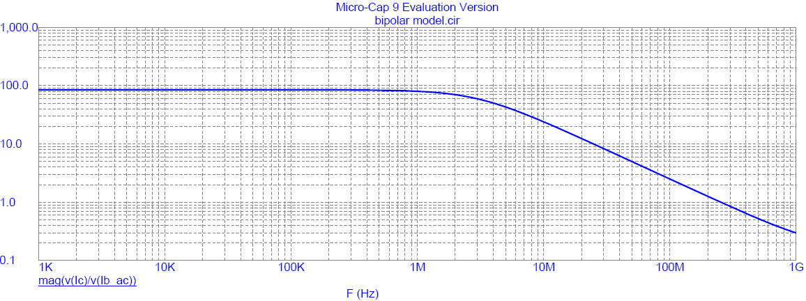
Now let's look at the variation in Transconductance Gm with frequency for the same base bias current of 25 µA. This should also fall off with frequency, somewhere between the -3 dB Hfe fall off point and FT . (The graph is scaled to Gm in mA/V and Gm = 50 mA/V at IC = 2 mA - This is a bit low!)
Well this hasn't happened - Gm increases at 1 GHz! What is wrong with MicroCap's bipolar model?
The model parameters in MicroCap show the base spreading resistance Rbb to be RB = 0 Ohms and the emitter spreading resistance Ree to be RE = 1.999923 Ohms. These physical silicon interconnection resistances are obviously wrong. The Rbb term forms a low pass filter with the base emitter capacitance (much larger than the zero bias value!) and would make Gm fall off with frequency. Also the Ree term represents a negative feedback, explaining the lower Gm than expected.
The 2N2369 will probably have a base spreading resistance closer to 25 Ohms. I changed the model parameter to RB = 50 Ohms and then did a new sweep.
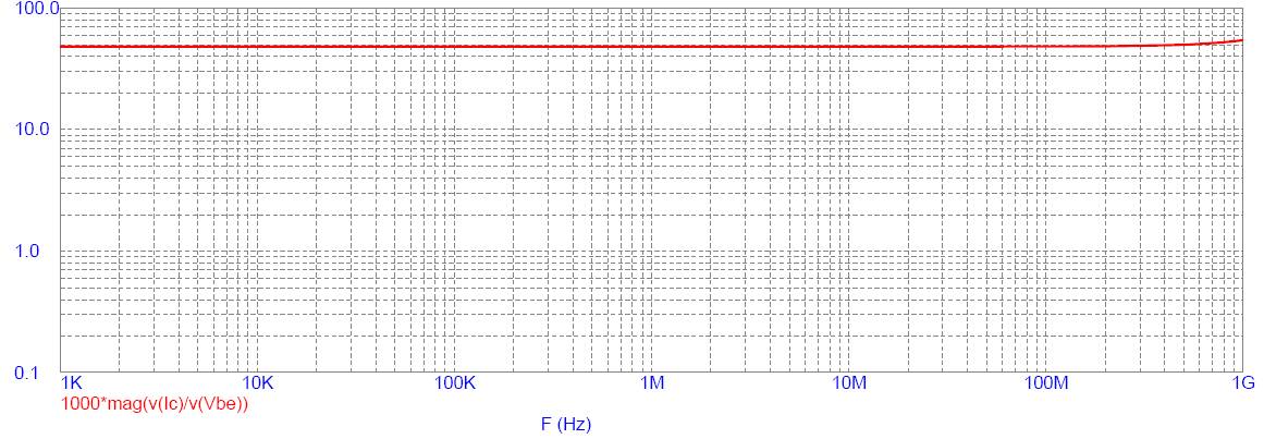
Notice that the small signal current gain Hfe is unaffected as expected, but the -3 dB fall off point for Gm is now closer to 100 MHz. This is far more believable!
Note: The term Rbb can be inferred from published Vbe versus IC data and affects power gain at high frequencies. It also directly affects Noise Figure in a predicable manner.
This "Transient Analysis" feature in MicroCap produces an oscilloscope output. The AC signal stimulus was set to 10 µA peak as a sine wave input to the base of the transistor. This was superimposed on the injected DC bias of 25 µA.
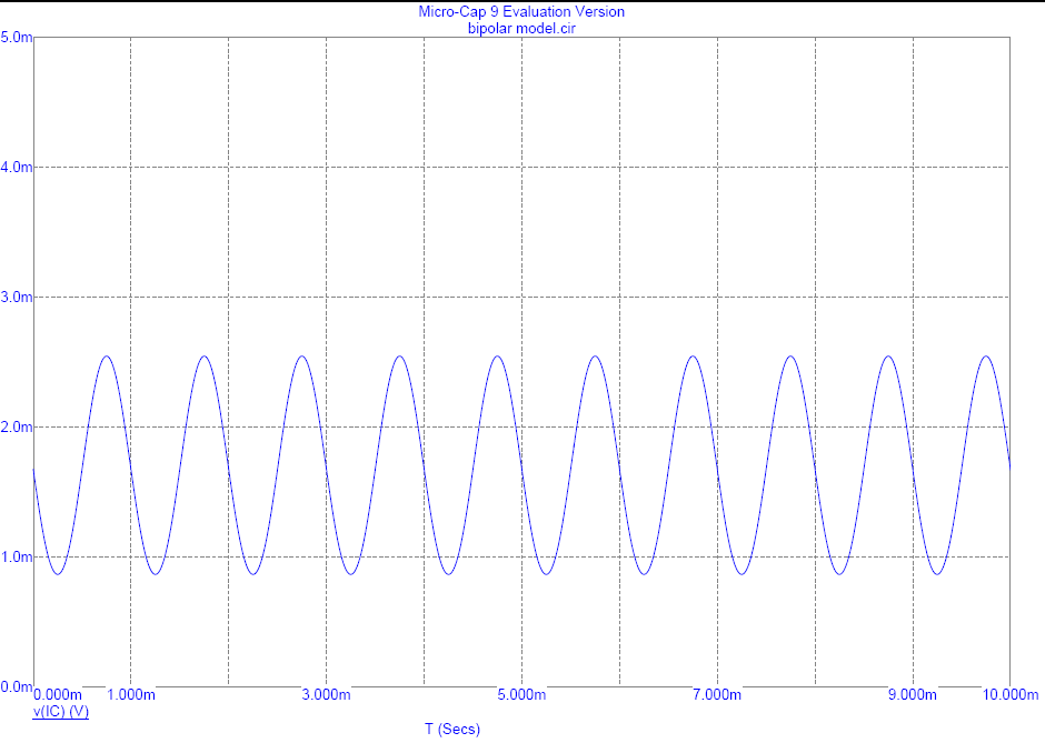
The collector current IC is displayed directly in mA and shows an average bias value of about 1.7 mA (i.e. HFE = 68). The peak to peak variation is about 1.4 mA or 0.7 mA peak, corresponding to 10 µA sine wave AC drive multiplied by Hfe = 68. Also the test frequency was 1 kHz, corresponding to a time period of 1 ms as shown.
The time domain waveform can now be converted to the frequency domain using MicroCap's internal FFT feature. The next graph shows a spectrum analyzer view.
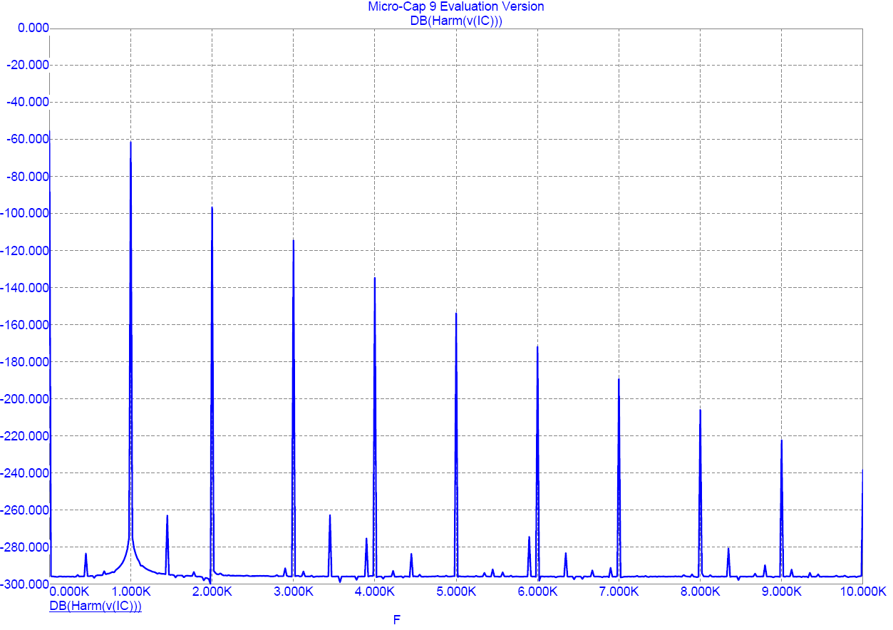
I set the y axis to decibels to show the dynamic range possible with this. This is about 300 dB - far in excess of any hardware test equipment! The DC term is shown with the fundamental AC term at 1 kHz slightly lower. The second harmonic at 2 kHz is about 38 dB lower again (1 %) and the third is about 18 dB further down again.
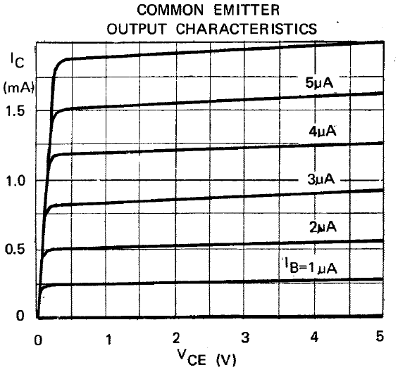
This graph is set up to show HFE on the y axis and collector current IC in mA on the x axis. There are four curves showing VC = 2.5 V, 5 V, 7.5 V and 10 V.
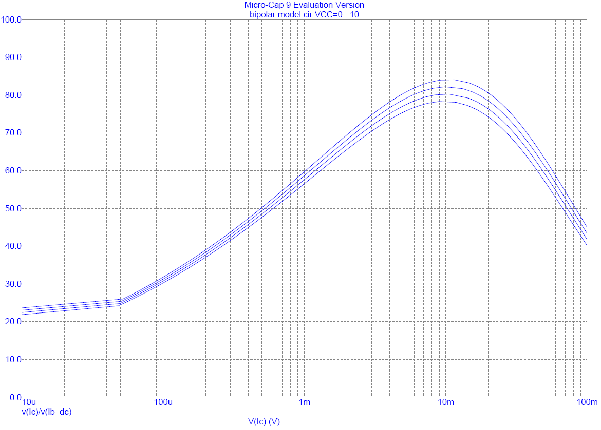
The DC current gain HFE shows a peak at IC = 10 mA of about 85 times. The current gain at IC = 2 mA is about HFE = 70 in agreement with previous analysis outputs.
The model parameter for HFE in MicroCap is BF = 199.979753. The "shape" of the curve is modified in a complex way by the "I" terms such as IKR (high current corner) etc. Admittedly not "scientific" it is fair to say that "tweaking" these parameters can modify the results to match published data to an adequate level. Once again, transistor parameter spreads are massive, so even approximate models will probably be fine.
Transistor data sheets contain a lot of information that is often unused by design engineers. This web topic will show how to use this data to obtain many transistor parameters directly, and how to incorporate these into device parameters used in simulation software such as MicroCap. This "extraction" procedure is relatively simple and reasonably accurate (and certainly better than having no extraction method at all!)
To begin, we need to start with some basic semiconductor diode theory and mathematics.
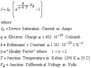
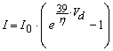
The semiconductor diode has a characteristic equation that has been theoretically and empirically derived to closely approximate the following equation, relating its terminal voltage to the current flowing.
 ...(1)
This equation predicts diode current in forward bias (Vd > 0 V) and reverse bias (Vd < 0 V) regions, but does not include process imperfections such as "leakage current" and "series resistance" etc. However it represents a good starting point for extracting some of these imperfections from published DC data sheets. It does include a "fudge factor" represented by an "ideality factor" n that refers to the actual availability of electrons and holes in the semiconductor material. Its actual value does affect final transistor Transconductance Gm and lower values (closer to 1) provide greater Transconductance.
We can group most of the coefficients in equation (1) to produce a simpler equation
 ...(2)
Equation (2) will now be used to extract the "base spreading resistance" parameter Rbb referred to as RB in MicroCap's bipolar device library. Bipolar transistors operate when the base-emitter junction is forward biased. Since this is a diode junction, its characteristics must be defined as per equation (2). Silicon diode junctions typically have forward biased voltages around 0.7 V depending on device physical fabrication details, operating temperature and current (Other semiconductors such as germanium have different "typical" forward voltages such as 0.2 V or gallium arsenide, approximately 1.3 V). The exponent ional term (in all cases) tends to be extremely large compared to the "-1" coefficient and so can be discarded for the purpose of parameter extraction. This results in a further simplified equation given by
![]() ...(3)
...(3)
We can use equation (3) to get a reasonably good estimate from transistor data sheets using the "forced beta" VBE data (sometimes referred to as "saturated" VBE data). An example graph taken from the popular BC549 transistor series shows (Micro Electronics data sheet)
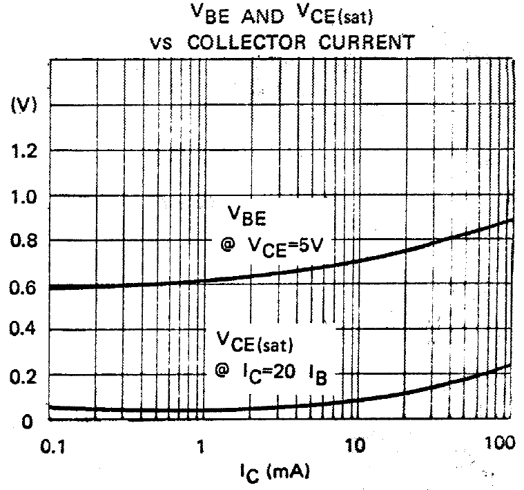
This graph shows VBE under normal conditions and VCE "forced beta" data. Forced beta represents a condition where the transistor collector current is held constant at a specified level and the base current is increased to a specified ratio of this. This causes "transistor saturation" and the collector voltage falls to it's lowest possible value. This condition is preferred because the device base current is exactly known for each collector bias current. For example if IC = 100 mA and the forced beta HFE, forced = 20, we know that the base current IC = 5 mA. Unfortunately this graph only shows forced beta conditions for the collector to emitter saturation voltage VCE, forced and the actual base emitter bias voltage is shown under normal operating conditions. In this case, the base current IB would equal IB = IB / HFE . This data can still be used of course, but the additional parameter HFE must be included and this is current dependent (i.e. a minor additional hassle in the parameter extraction procedure). Thankfully, the data sheet does contain tabulated data for VBE under forced beta conditions and we will use this for less problematic demonstration

In order to derive the base spreading resistance Rbb and other resistive terms Ree and Rcc we need to consider the physical geometry of the bipolar transistor. The actual "active" transistor is nested inside the structure where the base region is thinnest. Currents flowing into its terminals pass through parasitic semiconductor resistance causing additional voltage drops. These voltage drops show up in the published DC data as deviations from the theoretical voltage drops that would be expected from equation (3).
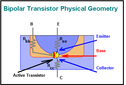
Based on semiconductor area, we can expect the collector parasitic resistance Rcc to be small and with the emitter parasitic resistance Ree slightly larger. The base spreading resistance "channel" for Rbb is much thinner so its resistance will dominate.
Step 1. Estimating Ree and Rcc
We note that VCE, forced shows a "plateau voltage" that remains constant across a wide range of collector currents. This appears to have a minimum at VCE, forced = 0.2 V when IC = 1 mA (for this transistor). Now consider V at a much higher current, e.g. IC = 100 mA. We can attribute this increase in voltage due to the contribution caused by R and R combined. The difference in voltage is 0.2 V at IC = 100 mA, so we conclude that Ree and Rcc could be estimated as Ree + Rcc = 0.2 V / 0.1 Amps = 2.0 Ohms. (we will assume the emitter current and collector currents are sufficiently equal)
The issue is now which is which? Although an "exact" procedure could be derived, it should be remembered that this exercise is intended to provide adequate data for circuit simulation when no other device models are available. For the purpose of illustration we will simply suggest that the emitter resistance is slightly larger and assume than Ree = 1.5 Ohms and Rcc = 0.5 Ohms. Of these terms, Rcc will have little effect on device amplification whereas Ree has a much larger affect. These two parasitic terms affect saturation voltages equally, so this "thumb suck" estimation is probably adequate for now.
Consequently we will define Ree = 1.5 Ohms and Rcc = 0.5 Ohms for this BC549 transistor model.
Step 2. Estimating The Base Spreading Resistance Rbb
The base spreading resistance Rbb can be estimated but only approximately, in part because it is not constant with collector current and also because its estimation is based on a subtraction between two similar voltages. MicroCap, for example, includes a model parameter "IRB" defined as "the current at which RBB = one half". Therefore we can only obtain a better estimate than simply setting Rbb = 0 Ohms which the available MicroCap models seem to do (This will cause large simulation errors for high frequency predictions).
It may be of interest however, to make a prediction and to understand some of the mathematical derivation behind a prediction formula. I will offer a simplified derivation in this topic, and then use it to make some predictions.
Let us return to equation (3) and make the forward bias voltage the subject
![]() ....(4)
....(4)
Equation (4) predicts the forward bias voltage V for a forward current I based on an "ideal" diode junction. If we include the additional voltage drop caused by some parasitic series resistance we have a modified equation given by
![]() ...(5)
...(5)
Now consider this forward voltage drop prediction at two different currents I1 and (a larger) I2 corresponding to voltages V1 and V2.
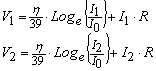 ...(6)
This represents two simultaneous equations that we want to solve for the parasitic resistance R. However the equations are non linear and an exact solution is (?) impossible. However if we choose I1 to be adequately small we can simplify the equation
 ...(7)
Equation (7) can now be solved easily to produce the following result
 ...(8)
We now see the potential for large estimation error caused by the subtraction of two voltage terms with possibly similar values. Also, the "ideality factor" n is unknown, but tends to be closer to n=1 than n=2 (it can presumably be derived also from published data at lower current ranges - actually this whole procedure could probably suit a small MATHCAD file!)
Let us use the tabulated data directly, i.e. Vbe = 0.7 V at Ib = 0.5 mA and Vbe = 0.9 V @ Ib = 5.0 mA. This implies
dV = 0.2 Volts
I1 = 0.0005 Amps
I2 = 0.005 Amps
=> R = 28 Ohms if n = 1
But is this the real value for Rbb ? Note that the emitter parasitic resistance term Ree ~ 0.15 Ohms causes an additional voltage drop of Vee ~ 0.15 V at Ic = 100 mA. This would reduce dV to 0.05 V and a corresponding revised estimate for R = -2.0 Ohms!
This negative resistance term is clearly non physical and demonstrates that the model "breaks down" significantly (at high currents). Indeed, MicroCap tends to set Rbb = 0, however this is equally invalid. Perhaps the non saturated data can be used?
| Collector Current
Ic mA |
HFE at this collector current | Base Current
Ib µA |
Forward Voltage Drop
Vbe Volts |
Estimated Rbb
Ohms |
| 1.0 | 290 | 3.5 | 0.61 | 1,200 |
| 10.0 | 310 | 32 | 0.71 | 21 |
| 100.0 | 160 | 625 | 0.9 | 272 |
Well I guess I must be telling porkies! One suggestion may be that the current flow is also lateral (across the face of the base-emitter junction) and this diode junction "section" has a low effective series resistance path. The longer resistive path to the active transistor site may be masked by this lateral current path, as it would appear "approximately" in parallel.
Well I got annoyed at this approach so I decided to measure a transistor myself. I took a BC549 from my junk box and measured its base emitter forward voltage drop using a multi-meter and left the collector open - so that only the base emitter junction was under measurement. Here are the results
| Direct Base Current
Ib mA |
Forward Voltage Drop
Vbe mV |
Forward Voltage Drop
Vbc mV |
Forward Voltage Drop
Vbc,e mV |
Estimated Rbb
Ohms B-E |
Estimated Rbb
Ohms B-C |
Estimated "Amplified Transistor" Rbb
Ohms C+B - E |
| 0.1 | 652 | 647 | 584 | 58 | 49 | 13 |
| 1.0 | 770 | 756 | 657 | 27 | 39 | 13 |
| 10.0 | 1046 | 1158 | 837 | 22 | 34 | 12 |
Now we are getting somewhere but the measured data is curious to say the least. Direct measurement of "Rbb " ranges from 22 Ohms to 58 Ohms. Note that this "resistance" includes lateral current flow in addition to the current expected to reach the active transistor site. It therefore must represent a "lower bound" to Rbb. (Actually, this base spreading resistance is probably a "ladder network" rather than a single discrete resistance as shown in my previous diagram!) My guess is RB=100 Ohms to the active transistor site.
What has been established from this is that Rbb is definitely non zero. Older data sheets on RF devices often infer its value it at an RF test frequency from a time delay factor when combined with the collector - base capacitance of the transistor. Without such data, we are possibly best advised to use a value of Rbb on the higher side for the model parameters, and check that low frequency behavior is not affected by this. The higher frequency behavior will however benefit in accuracy (for example, Transconductance would not increase above the device FT !)
An "ideal" bipolar transistor would have a current amplification ratio HFE that remained constant for all collector currents Ic. This however is not possible. Real bipolar transistors show a maximum HFE at some mid range collector current and this value falls off at low and high collector currents. The published "Philips BC549" transistor data sheet presents the following graph.
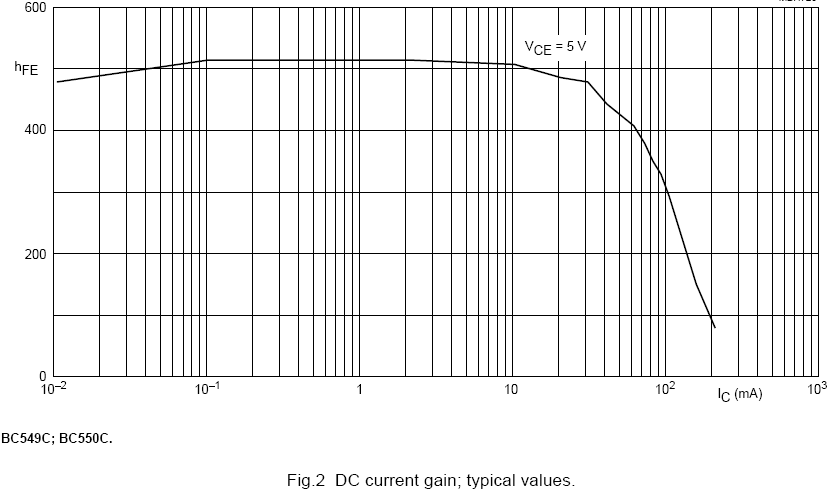
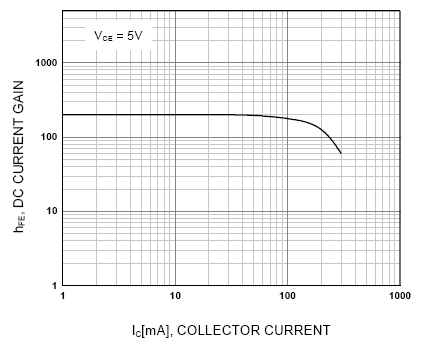
This graph shows a maximum HFE = 510 at Ic = 1 mA, falling down to HFE = 100 at Ic = 200 mA (its maximum peak current rating) corresponding to a percentage ratio of 19.6 % and to HFE = 480 at lower currents Ic = 10 µA. Interesting the "Fairchild BC549" shows a slightly different profile, presumably based on a lower HFE grade device. Unfortunately the low current region is not shown but the high current region shows a deterioration in HFE from its maximum value of HFE = 200 to HFE = 120 at Ic = 200 mA. This shows a fall-off of only 60 %. Obviously not all BC549's are the same!
Now let's look at apparently old published data for the "Micro Electronics BC549".
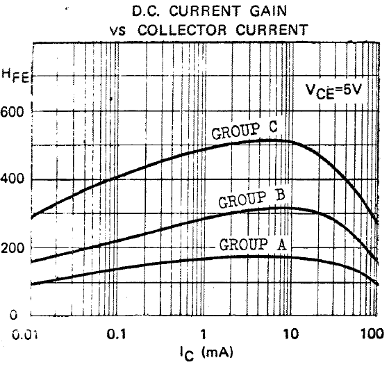
The high gain group shows HFE = 290 at Ic = 10 µA, a maximum HFE = 510 at Ic = 5 mA and HFE = 270 at Ic = 100 mA. The "Philips BC549 has HFE = 300 at Ic =100 mA). This time the high current fall-off ratio is much the same, but the low current fall-off is much worse.
These variations can show up sometimes when transistors are replaced and the modern version behaves differently than the older version. Modern transistors benefit from better manufacturing process control but some older products may have inadvertently made favorable use of a detrimental characteristic.
I hope these demonstrations so far illustrate that the need to "exactly" extract model parameters may well represent a fruitless journey. What can be done though, is to test a given circuit with various "versions" of a target transistor based on variation in its parameters. A good design will be tolerant of this, a bad design will be critical.
So with this philosophy in mind, what parameters affect the "shape" of this curve in MicroCap (and other SPICE based simulators).
To demonstrate this parameter control consider the following table of MicroCap device model parameters (Bold entries affect HFE ).
| BF
Forward Beta |
IKF
High Current Corner |
IS
Saturation Current |
ISE
B-E Saturation Current |
ISC
B-C Saturation Current |
RB | IRB
Current at RB=Half |
RBM
Minimum RB at High Currents |
RE
|
| 400 | 0.1 | 1e-11 | 2e-12 | 1e-11 | 150 | 0.01 | 0 | 1.5 |
| 400 | 10 | 1e-11 | 2e-12 | 1e-11 | 150 | 0.01 | 0 | 1.5 |
| 400 | 0.1 | 1e-11 | 0.5e-12 | 1e-11 | 150 | 0.01 | 0 | 1.5 |
The parameter BF determines the maximum HFE possible, but other fall off parameters may prevent the full value. The second parameter IKF represents the high corner collector current (in Amps) where HFE is one half. The first rows sets this corner to Ic = 100 mA. The third column IS represents a "general" semiconductor saturation current (I think) in accordance with equation (3). The low current corner for HFE is determined by ISE. Higher values cause a greater fall off in HFE at low collector currents. It appears that ISE must be less than IS.
ISC appears to have no effect. RB affects high frequency behavior for Transconductance. IRB illustrates the phenomenon we found earlier where Rbb appeared to be poorly predicted from published data. RBM sets a lower limit, presumably to prevent negative values! Finally, RE sets an upper limit to Transconductance (i.e. Gm < 1/ RE) and contributes to collector emitter saturation voltage.
Row 1 - BC559 PNP Example With Low End Fall Off and High End Fall Off
Row 2 - Removing The High Current Corner (Can also set IKF=0 to remove this corner)
3. Removing The Low Current Corner
This parameter describes "effectively" the maximum voltage gain that the bipolar transistor can achieve. Notice that the previous MicroCap curves had VAF = 200 V resulting in a variation in HFE, and therefore collector current Ic for changes in collector voltage from 2.5 V, 5.0 V, 7.5 V and 10.0 V.
It follows that a large variation would possibly "compete" with an output voltage swing, whilst zero variation could result in an infinite output voltage swing for constant collector current.
VAF is current dependant but can be found by extrapolating the "straight, near horizontal" curves below down to the left hand side of the x-axis. The x-axis value equals VAF.
Typical values are VAF = 200 V. Lower values represent "more vertical lines" and effectively a lower output resistance in the transistor. This is equivalent to lower voltage gain potential. Setting VAF=0 removes this model parameter in MicroCap.
Semiconductor diodes have a reverse biased voltage dependent junction capacitance that tends to agree with the following equation
 ...(9)
The coefficient C0 represents the "zero bias" capacitance and "alpha" represents a "grading factor". The term VF is usually 0.7 V and is associated with a typical silicon diode's forward voltage drop. MicroCap applies this equation to the Base-Emitter junction and the Collector-Emitter junction.
The Collector - Base junction uses CJC to represent C0 and MJC to represent "alpha". Similarly, the Collector-Emitter junction uses CJE to represent C0 and MJE to represent alpha.
The "Philips BC549" tabulates Cbc = Cc and Cbe = Ce as

The "Fairchild BC549" tabulates Cbc = Cob and Cbe = Cib as

Once again, despite different notation conventions, these are two different transistors! Further, the "Micro Electronics BC549" only presents Cob as
![]()
It has been said that a simulation is only as good as the device model data you use. Actually the device data may only be as good as your simulation!
![]() ...(10)
...(10)
The "grading coefficients" however are far less device dependant and are determined by the "steepness" of the semiconductor junction. Gradual doped junctions have the lowest alpha usually close to alpha = 0.333. Sharp doping profiles result in higher alpha values suitable for varicap diode applications. Hyper abrupt diodes continue this trend further with values approaching unity. Bipolar transistors never seem to have abrupt junction profiles, so alpha=0.333 is standard.
From the "Philips BC549" data we set MJC = MJE = 0.333 into equation (10) and predict CJC = 3.7 pF and CJE = 10.8 pF for each reverse voltage indicated as Vcb = 10 V and Veb = 0.5 V.
The parameter CJC represents a collector to base negative feedback path and therefore reduces the transistor's power gain at high frequencies. (It has little effect at audio frequencies). The parameter CJE reduces the device FT at low currents. Bipolar transistors tend to show a current dependent Transition Frequency FT as
The "forward transit time" parameter TF is closely related to the transistor's Transition frequency FT according to
![]() ...(11)
...(11)
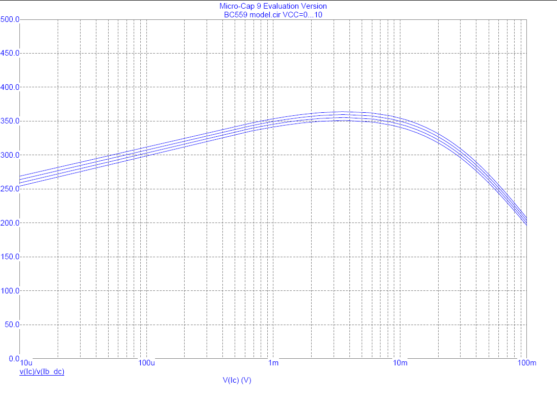
Let us assume the "BC549" transistor has FT = 300 MHz at Ic = 10 mA . This would predict that TF = 530 ps. The resulting Transition frequency FT is represented on the following graph where Hfe = 1. We correctly observe that the cross over point is indeed equal to 300 MHz!

Now lets run the simulation at Ic = 0.1 mA, based on the use of the previous extracted model parameters (Philips case).
We see that the unity current amplification cross over occurs at 38 MHz, i.e. FT = 38 MHz at Ic = 0.1 mA.
The Philips BC549 data shows FT = 38 MHz at this bias current - not too bad for some very simple extraction procedures from published DC data!
It may be of interest to continue this topic based on a new circuit file that allows better control of collector bias current and resulting small signal AC behavior
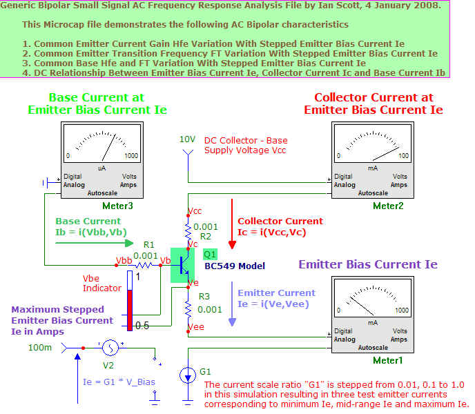
This circuit file biases the NPN (or PNP by changing polarity) as a "common base" configuration but uses the various terminal currents to predict AC small signal behavior in common emitter as well as common base. These parameters are defined as common base amplification ratio Hfb = d Ic / d Ie and common emitter current amplification ratio Hfe = d Ic / d Ib where the "d" refers to "change in". The actual "injection point" for the AC generator is unimportant and these current ratios are independent of this. Now let's plot the frequency response for Hfb and Hfe for three stepped emitter bias currents (1/100th, 1 /10th , and 1/1 ) .
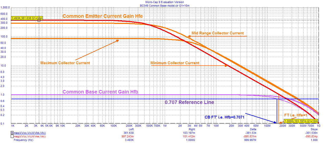
We observe that H and H are both current and frequency dependent. Of some interest is an error that most text books on electronics seem to perpetuate. This refers to the relationship between the common emitter Transition frequency FT,CE and the corresponding common base "cut off frequency" FT,CB ). The common base cut-off frequency FT,CB is defined as the frequency where the common base amplification ratio falls to 20.5 ~ 0.7071 of its low frequency value and that
FT,CE = FT,CB .... note the MicroCap simulation shows a small difference between these two parameters.
This "error" has occurred (I suspect) because Hfe and Hfb were added in exact phase quadrature i.e.
Ie = Ib + Ic
= Ic · [ 1 + 1 / Hfe ]
i.e. Hfb = Ic / Ie = (1 + 1 / Hfe )-1
Now Hfe = | Hfe | · e j · Ø
The magnitude of the common emitter current gain | Hfe | = 1 at the Transition Frequency FT but will the associated phase Ø be exactly -90 degrees at this frequency? (If this is true, then Hfb = 1 / ( 1 - j ) i.e. | Hfb | = 2-0.5 but perhaps Ø has some "excess phase")
Note: Summary & Additional Model Parameter Extraction Information
| MicroCap Model Parameter | Derivation Method | Definition and Importance |
| BF | HFE (maximum possible value in model) | Actual "peak" HFE, peak may be less than this depending on other parameters |
| IKF | Collector current where HFE = 1/2 of HFE, peak | From published HFE versus collector current Ic data graph |
| NF = 1 implies that | k = 38.93 at T = 298K , equation (1) | From Boltzmann's constant and electron charge in equation (1) |
| NF > 1 | k/ = Loge { Ic2 / Ic1 } / [ Vbe2 - Vbe1 ] | Actual value taken from two mid range values of Vbe and Ic in published data |
| NF = n | n = k / k/ ( n > 1) | The "forward emission coefficient" NF reduces transistor Transconductance |
| NC = NE = 1 | NE will interact with ISEnote | TBD "forward emission coefficients" for BE and CE junctions |
| IS | IS = exp { [ Vbe2 · Loge { I1 } - Vbe1 · Loge { I2 } ] / [ Vbe2 - Vbe1 ] } | Common emitter "saturation current" taken from two mid-range values of Ic and Vbe |
| ISC | Has very little effect | |
| ISE | 0 <= ISE << IS | Base-emitter "saturation current" - increase this value to make HFE fall off at low currents |
| VAF | 100 < VAF < 200 | Forward Early Voltage - High values reduce collector current variation with voltage Vce |
| TF | TF = 1 / [ 2 · pi · FT ] , affects rise and fall times | Forward "Transit Time" derived from Transition Frequency FT |
| TR | TR >> 100 · TF , affects storage time Ts | Charge storage time for saturated switching, much larger than TF |
| BR | BR ~ 1 | Reverse HFE - (collector and emitter swapped) - actual storage time reduces as BR increases (inversely proportional) |
| IBR | IBR > 0 | Current scale factor for BR - small values increase BR and storage time |
| MJC = MJE | MJC = MJE = 0.33 | "Grading coefficient" for varicap diode equation - fairly consistent |
| VF | VF = 0.75 | "Junction potential" voltage for varicap diode equation, default value |
| CJC | CJC = Ccb { Vcb } · [ 1 + Vcb / VF ]MJC | Zero bias collector-base capacitance derived from Ccb at a bias voltage Vcb |
| CJE | CJE = Ceb { Veb } · [ 1 + Veb / VF ]MJE | Zero bias emitter-base capacitance derived from Ceb at a bias voltage Veb |
| RE + RC = RT | RT = [ Vce, sat / Ic, sat ] | Total transistor resistance from sum of emitter and collector contributions |
| RC | RE = 1/4 · RT | Approximate "guessed" ratio for Rcc as collector junction area is larger than the emitter area |
| RE | RE = 3/4 · RT | Approximate "guessed" ratio for Ree as emitter junction area is smaller than the collector |
| RB | 0 < RB << 100 · RT | Approximate "guessed" ratio for Rbb , potentially large as the "active transistor" base is buried deep in the transistor structure |
These approximate relationships were determined with a mixture of reason and experimentation and therefore are not rigorous. The methodology does allow reasonable starting point for a model, especially if MicroCap does not have the required transistor (or near equivalent) in its bipolar model library.
One observation that may be useful for bipolar operation at low currents relates to IS, NF, ISE and NE. It appears that Ic = IS · ek · Vbe / NF where k = 38.93. However the base emitter current is "shared" with a parallel diode defined with corresponding model parameters ISE and NE (perhaps lateral current flow across the transistor die?). If we set ISE = IS and NE = NF the model will show a current gain HFE ~ 1 (i.e. a "current mirror"). Further if ISE = IS / 10 then HFE ~ 10. These two terms "act like" resistors in parallel i.e. HFE ~ [ 1/HFE, peak + ISE / IS ]-1 .
Now the effect of low current operation on HFE can be adjusted by increasing NE > NF. The low current fall-off in HFE can be controlled by increasing ISE and NE.
From the previous reasoning, the BC549 model data I currently use is
| RE | RC | RB | BF | IKF | IS | ISE | ISC | IRB | RBM | VAF | CJC | MJC | CJE | MJE | TF |
| 1.5 | 0.5 | 100 | 400 | 0.1 | 1e-11 | 2e-12 | 1e-11 | 0.01 | 0 | 200 | 3.7p | 0.333 | 10.8p | 0.333 | 530p |
| Vce, sat | Vce, sat | guessed | HFE, max | High Ic corner | Typical | Low Ic
corner |
minor effect | Half RB | Min RB | Voltage Gain | Ccb @ Vcb=0 | Typical | Cbe @ Veb=0 | Typical | FT |
It is possibly useful to include a demonstration of large signal analysis in this web chapter. MicroCap (student) provides a useful level of time domain analysis capability that can be applied to various high speed switching circuits. The previous parameter extraction procedure allows reasonable functional behavior fron bipolar device models, but this can be further extended with a few additional parameters to also describe large signal, non linear behavior.
To illustrate this capability, please consider the following MicroCap circuit file
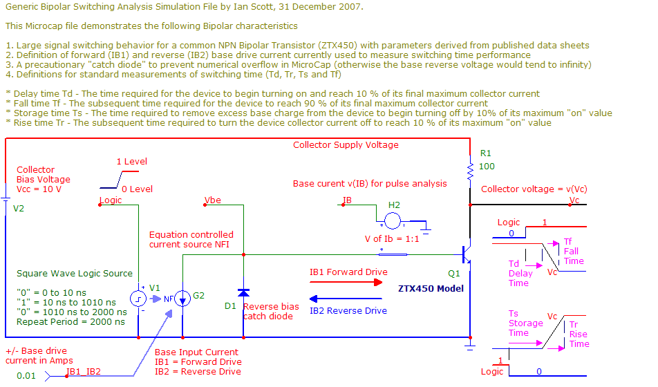
I have arranged this topology to allow a generic NPN bipolar transistor to be simulated as a saturated switch. This begins with a "0" to "1" logic generator describing "device off" and "device off" states. Although this logic source is effectively an instantaneous switch, a real bipolar device will exhibit a finite response time to this stimulus.
A logic level cannot be directly applied to a bipolar device (unlike a logic gate that is intended for this mode), so some interface arrangement is necessary. I have shown an "equation controlled current source", referred to in MicroCap as a "NFI" source, to provide suitable scaling and DC offsets according to
IB = IB1_IB2 · 2 · [ v(Logic) - 0.1 ]
IB1 refers to a positive drive current into the base of the NPN bipolar transistor under simulation (causing it to turn on) and IB2 refers to a negative "withdrawal" current intended to reduce the device turn off time. The two current are usually listed in published device data sheets as having equal magnitude, but NFI can be modified to set each independently (just add another term in the equation and use another DC control (shown with IB = 0.01 in the schematic).
I modeled the popular ZTX450 1 Amp NPN switching transistor following the previous procedure and added a TR parameter to include "charge storage time". The 100 Ohm collector resistor, combined with the 10 Volt supply defines a maximum collector current of Ic = 100 mA (Vce > 0 V ) and a minimum collector current of Ic = 0 mA (Vce < 10 V). The output collector voltage Vc is monitored, but the base voltage Vb and actual base drive current Ib can also be monitored as shown)
Of note is the inclusion of the "catch diode" D1. Since the drive source has a bi-polar current output, negative charge extraction will eventually drain all current from the device' base and it will become reverse biased. This state represents a high impedance and can lead to simulation failure in MicroCap (numerical overflow). The catch diode "clamps" the maximum reverse bias to about -0.7 V.
The transient simulation provided the following collector voltage waveforms combined with the logical drive generator.
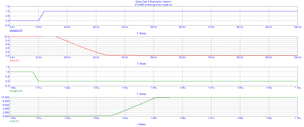
The top graph shows the logic source transition from "0" to "1". The second graph shows the "turn on" delay Td, followed by a gradual fall in collector voltage as the device turns on, i.e. it's "rise time" Tr. In this example the delay time Td is approximately 5s, followed by a rise time Tr of approximately 20 ns. (These are usually defined as 10 % - 90 %)
The third graph is moved along the time axis to show the logic source transition from "1" to "0". This shows a longer turn off time consisting of a "storage time" Ts of about 25 ns followed by a "fall time" Tf of about 15 ns. The length of this storage time Ts is controlled by the parameter TR in the device model but not directly.
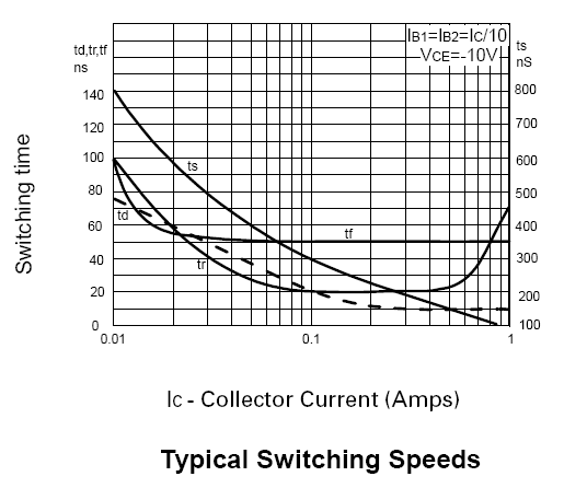
To be fair, this is a useful feature to include but it only approximates real device behavior. Real bipolar devices have current dependency in all parameters whilst the simulation model does not reflect this. For example, the ZTX450 data shows Ts = 300 ns at Ic = 100 mA and Ts = 80 ns at Ic = 1 Amp.
These web chapters have indicated some of the software simulation tools that are available to the amateur experimenter. MicroCap student version has been used because this is free for use by students. Despite its limitations, it is still capable of in depth analysis of active components, shown through the use of a bipolar transistor example.
One limitation in the student version is its relatively small component library (often including transistors that may not be considered to be available). However the use of a circuit modeling file allows a similar transistor to be "tweaked" to match a wanted variety using reasonably straight-forward manual methods.
This model need not be extremely accurate as transistor parameters often vary two to one or greater between batches. Further, even MicroCap's 2N2369 model has been shown to have extremely suspicious device parameters leading to unrealistically high frequency Transconductance capability up to 1 GHz and higher! This however could be corrected by modifying a single device parameter relating to Rbb .
Even so, this web chapter has shown massive device parameter variation in published data from several manufacturers based on the popular BC549 series. This suggests that a pure or exact parameter extraction methodology is probably a waste of time and effort. After all a given circuit design should not be critically dependent on device characteristics. One value in the use of models is that device parameter spreads can be introduced in order to check that a given circuit design remains tolerant to these.
The old saying "you get what you pay for" is largely true, however MicroCap has shown that "what you get" isn't all that bad at all! It has limitations in the student version, but these can be largely circumvented with a bit of imagination, as shown.
I will show in other web chapters how far MicroCap can now be stretched - into high power RF amplification and even VCO phase noise analysis.
For students and hobbyist and amateur scientists that may be unable to afford a few million dollars to by ADS or Libra or Eagleware etc, the availability of free simulation software that can may have some limitations is not a bad compromise. With a little imagination and "tweaking" it can provide (at least) approximate predictions that will be far better than a "thumb guess" and certainly very suitable as an educational tool that demonstrates device and circuit behavior.
![]()
Return to Microcap Simulation
or Ian Scotts Technology Pages
© Ian R Scott 2007 - 2008