![]()
Mixed Signal Devices (MSD) combine Analogue and Digital processing elements in a single device. They are useful for signal acquisition (Analogue to Digital Conversion “ADC”) or signal generation (Digital to Analogue Conversion “DAC”) applications. As such they bridge the gap between the Analogue world and the Digital Signal Processing (DSP) world.
The Analogue world is characterised by continuous voltage and current waveforms. In contrast, Digital systems use discrete time sampling and operate with quantized values of equivalent signal representations. Consequently, each has very different behavioural attributes that require reconciliation in each MSD.
The advantages of processing signals in the digital domain include accuracy, repeatability and flexibility. In addition, some processing algorithms can be designed that have no equivalent in the analogue domain, or, for some that may, only implementations that are clumsy, expensive and inaccurate. Although Digital signals are quantized in time and numerical value, the extent of this quantization is known and invariant, as opposed to analogue signals that are affected by variable aberrations. These include frequency response errors, amplitude-phase non-linearity and random additive and multiplicative noise (e.g. VCO Phase Noise)
Despite the advantages of Digital Signal Processing, eventually some interaction with the outside (Analogue) world will be required. For example, speakers and headphones require analogue input signals and microphones produce analogue signal outputs. Equally, light requires analogue transducers, either as Charge Coupled Devices (CCD’s) used in cameras, or LED based computer monitor screens. Other analogue signal types include temperature transducers, motion detectors, smoke detectors and devices for chemical composition analysis. These all require an analogue signal interface, and some additional analogue signal processing, but the current industry trend is to minimise the analogue hardware overhead in favour of extended digital processing capability. The interface between these two domains can be referred to as Mixed Signal Devices (MSD) that bridge the gap between two very different worlds, so that activities in each can be optimal.
In the “real world”, quantities such as temperature, position, size, weight, etc can be considered to have infinite fine graduation in their values. However, we equally associate the value of any particular item with a cost that can only take on discrete values. European currency is counted in cents, therefore European currency is quantized in units of 1 cent.
A bit resolution of 1 refers to the case where a coin, as in the previous example, is either present or not present. Its “value” is therefore 1 if present or 0 if absent. Its value “x” can therefore be represented as
![]() …(1)
…(1)
One bit converters are used for simple yes/no requirements, and in some audio applications where extreme over-sampling is used to effectively increase the number of Bits (refer to topic on decimation).
Multiple Bit MSD’s are desirable for RF applications as they provide good Bit resolution with minimum sample frequency requirements. A N-Bit value is represented as
![]() …(2)
…(2)
For example, a 2-Bit word (N=2) has possible values of 0, 1, 2 and 3. A 3-Bit word (N=3) has values of 0, 1, 2, … 7. In other words, A N-Bit word has quantized values of 0, 1, 2, … 2N-1.
For DC applications, The Bit value may start at 0, but RF and IQ applications usually require ± x value representations. In this situation a simple DC offset is added to the Bit-word, and equation 2 becomes,
 …(3)
…(3)
Analogue signals operate in a continuous time domain, but digital systems require that the signal is sampled at discrete time intervals. This sampling is usually performed at a constant rate referred to as the sample frequency Fs. This “snap shot by snap shot” view allows digital processing components such as Micro-processor, DSP, and FPGA’s devices to construct and analyse signals on a clock cycle by cycle basis.
No information is lost providing the Sampling Rate exceeds twice the bandwidth of the signal that is sampled.

In this example, a semi-sinusoidal signal is sampled at a low sample rate (stem plot) and a much higher sample rate (continuous plot). The captured signal value coincide for both cases, but it will be shown later that the lower sampled version will be less accurate than the higher sampled version. This is because the non-linear exponential-sin function has spectral content that extends to an indefinite frequency, but with diminishing energy content. As more of this energy is captured, the resulting accuracy improves.

Discrete time sampled signals have a repeating spectrum at integer multiples of ½ the sample rate Fs. Each even multiple can be described as a positive alias and each odd multiple as a negative alias.
![]()
Positive and Negative alias zones are
mirror images of each other joined at a vertical line centred at
![]() ,
,
![]() , …
, …
 where
where
 represents the highest wanted alias
frequency.
The alias zone
![]() for + and – alias versions, given
a target frequency component
for + and – alias versions, given
a target frequency component
![]() and sample frequency
and sample frequency
 is therefore
 …(4)
…(4)
where the function floor simply takes
the lowest integer approximation to its argument
![]() .
.
The first positive Nyquist zone is often
used for ADC and DAC operation. This mode is referred to as an
“over-sampled” application and sampled signals usually have spectral energy
components with frequencies that are significantly less than
![]() . However this zones limits a MSD’s frequency range to less than
. However this zones limits a MSD’s frequency range to less than
![]() and frequencies higher than the 1st
positive alias zone may require processing. This situation is commonplace for
ADC’s which can often capture signals that can be ten times or more higher
than their clock frequency. This operation is referred to as “sub sampling”
and no information is lost providing the bandwidth of the signal does not exceed
any given Nyquist alias zone.
and frequencies higher than the 1st
positive alias zone may require processing. This situation is commonplace for
ADC’s which can often capture signals that can be ten times or more higher
than their clock frequency. This operation is referred to as “sub sampling”
and no information is lost providing the bandwidth of the signal does not exceed
any given Nyquist alias zone.
The MAX1192 8 Bit ADC, for example, has a maximum clock frequency of 22 MHz, but can capture input signals as high as 400 MHz with minor performance degradation. In this example, a 400 MHz input signal would reside in the ADC’s 18th positive alias zone, i.e. covering the frequency range of 18*22 MHz = 396 MHz to 396+22/2 = 407 MHz.
From the previous example, we find
![]() . The 400 MHz signal, in the 18th alias zone will be equivalent to a
4 MHz signal is the first positive alias zone. After signal acquisition, the
effect of discrete time sampling makes any subsequent digital processing from
being able to determine which alias zone was utilized. Consequently the 400 MHz
captured input signal will be identical to a captured 4 MHz signal. Equally, a
414 MHz input signal will also produce 4 MHz as an alias, based on the ADC 18th
negative input alias response.
. The 400 MHz signal, in the 18th alias zone will be equivalent to a
4 MHz signal is the first positive alias zone. After signal acquisition, the
effect of discrete time sampling makes any subsequent digital processing from
being able to determine which alias zone was utilized. Consequently the 400 MHz
captured input signal will be identical to a captured 4 MHz signal. Equally, a
414 MHz input signal will also produce 4 MHz as an alias, based on the ADC 18th
negative input alias response.
When people are first introduced to
MSD’s they immediately assume that Bit resolution is some invariant quantity
based on the number of quantization bits
![]() and perhaps some minor
imperfections in the MSD. This assumption is completely false.
and perhaps some minor
imperfections in the MSD. This assumption is completely false.
Digital processing stages often use Variable Rate Processing (VRP) between successive processing stages in order to achieve more effective computational efficiency. An incoming signal may be sampled at a very high rate, and yet have very moderate signal bandwidth. It is only necessary to subsequently sample at a reduced rate based on this moderate bandwidth, after the signal has been captured (referred to as signal acquisition).
This process of down sampling is called “decimation”, and its equivalent up sampling process is called “interpolation”. In both cases, the signal’s bit resolution is altered.
Let us assume a 1 Bit ADC device (comparator) which has either a “0” or a “1” output state, operating at a sample rate of 40 MHz. Let us add, in the digital domain, each 4-group of output samples and produce a final result at the end of each 4 clock cycles. The output values will therefore occur at ¼ the incoming clock frequency, i.e. the output processed sample rate would be decimated by a factor of four.
If we add “0” and “1” output states over four captured samples, the output sums can only be,
Sums = 0, 1, 2, 3, or 4
If all captured samples had a value of 0 the sum would be zero. If all had a value of 1 then the sum would be 4. We see that we now have between 0 and 22 sates, similar to a 2 Bit word, even though the input was only a single bit. In other words, the process of decimation has caused some processing gain resulting in more bits but at a slower output sample rate.
Similarly, if we summed over 16 samples
and produced an output at
![]() the output rate, then the sum
outputs would range from 0, 1, 2, … 16, i.e. 24 = 16, i.e. 4 Bit
resolution for this decimation by 16.
the output rate, then the sum
outputs would range from 0, 1, 2, … 16, i.e. 24 = 16, i.e. 4 Bit
resolution for this decimation by 16.
(Note: why are there always 1 extra state?)
Interpolation is a reciprocal process and results in reduced Bit resolution at a higher output sample rate. No information is either gained nor lost in either process.
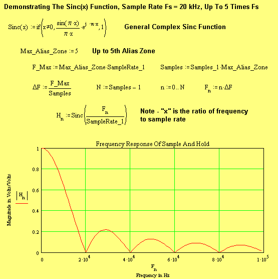
An infinitely thin time domain repeating
impulse signal has an infinite bandwidth and contains a train of repeating
alias’ at multiples of its repetition rate, each of equal spectral energy. In
contrast, a “staircase” pulse train has a repeating series of alias’ that
fall off in a “
![]() ” fashion. This
” fashion. This
![]() function is usually defined in the
frequency domain as,
function is usually defined in the
frequency domain as,
 …(5)
…(5)
The more general Complex frequency response for a sample and hold process is,
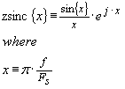 …(6)
…(6)
The magnitude response for equation (6)
is identical to that of equation (5), but an additional phase delay term is
introduced from the complex exponential
![]() .
.
So far we have shown signals that are sampled at an integer multiple of repetitive (periodic) frequency. When the Fourier Transform (FT) is applied, it assumes that the total analysis time begins from Time = -¥ and ends at Time = +¥. Obviously we may not that this much time to wait. However, waveforms that repeat in the time domain can be truncated to a single repeating period, and then processed with a FT. The frequency domain Nyquist zones then also repeat with equal alias. Providing the signal bandwidth is less than ½ the sample rate frequency then no information is lost from this truncation.
However, this exact repeating periodicity can only be achieved artificially, and most signals are only approximately periodic. We will refer to these as Non-Periodic. The effect of Non-Periodicity is to cause “spectral spillage” between FT frequency Bins.
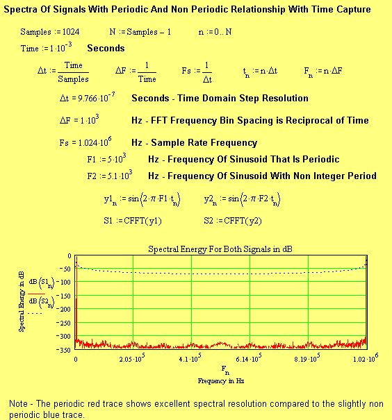
As can be seen, a small degree on non-periodicity has drastic effects on the FT spectral interpretation. The signal itself doesn’t, just its time domain truncated FT based interpretation.
Non periodic signals can be converted to approximate periodic versions by applying a time domain weighting to the signal before the FT interpretation. (The computer algorithm used to perform the FT is usually referred to as a FFT, or “Fast Fourier Transform”. It is identical in performance, but just computes the spectral coefficients in an efficient manner)
There are many possible window functions, but all attempt to force the start of the time domain signal to equal the last value, usually to zero. Any function that starts at zero when t=0 and ends at zero when t=Time can be multiplied by the input time domain signal to produce a version with the same properties. This forces the new signal to look periodic. However the process changes the signal and the trade-off is between overall dynamic range and nearby frequency resolution.
The simplest Window function is based on a ½ cycle cosine function defined as,
![]() …(7)
…(7)
Here
![]() represents the sample number
starting from 0, and
represents the sample number
starting from 0, and
![]() represents the total number of
samples (since we counted the samples from 0, rather than from 1.)
represents the total number of
samples (since we counted the samples from 0, rather than from 1.)
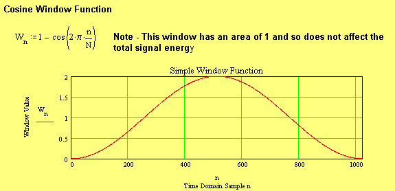
In general, the window function should be smooth, contain as much of the time domain signal as possible and be symmetric about its centre vertical axis. However the trade-off between amplitude dynamic range and close in frequency resolution cannot be avoided. The cosine window function covers on complete cycle, and so has a FFT Bin frequency of 1. When multiplied by the input time domain signal, adjacent “sidebands” will be generated around each spectral component. This is exactly the same situation that occurs in Amplitude Modulated (AM) systems. Sine the depth of this AM is 100 %, each sideband will be ½ the amplitude of the wanted component (analogous to a carrier tone), which will be seen as –6 dB on a decibel scale.
The cosine window can only generate adjacent sidebands, whereas other windows will generate adjacent, alternate and higher sideband components.
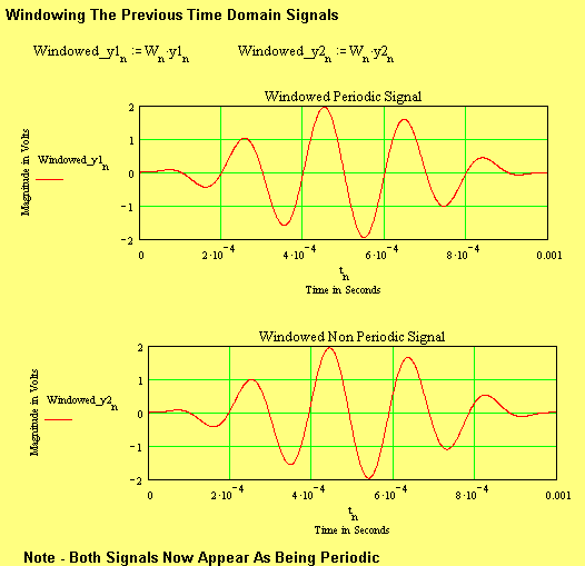
It might be thought that the windowing process is a bit “savage” to the wanted time domain signal, but it is merely an analysis tool that seeks to provide better spectral analysis for particular areas, usually to extend dynamic range at the expense of fine frequency resolution.
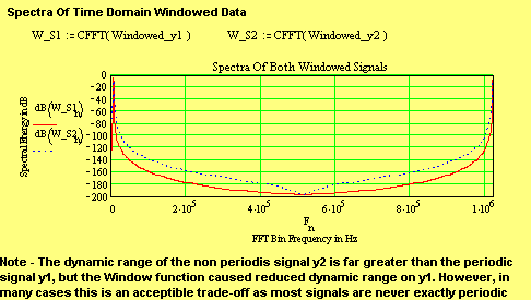
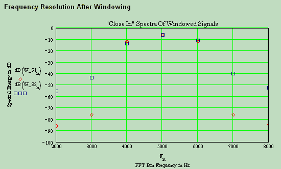
The red diamonds represent FFT Bin energy for the windowed
periodic signal, and the blue squares represent FFT Bin energy for the windowed
non-periodic signal. Both signals were sinusoidal with frequency of, and close
to, 5 kHz over a total analysis time of 10-3 seconds, i.e. the
corresponding FFT Bin separation will be 1000 Hz.
Both signals register spectral energy of –6 dB at 5 kHz, and about –12 dB on adjacent channels, as previously explained (AM effect). However some additional spillage still occurs at FFT Bins beyond the adjacent FFT Bin spacing. This is because a signal that ends at the same place it begins is not exactly periodic. Instead the last sample point should be discarded as this would be the first sample of the next concatenated time domain block.
All MSD’s have a maximum voltage, current or power limit, referred to as “Full Scale” or FS. Signals below FS are quantized according to a given Bit resolution. A typical ADC will have a FS input range between ± 0.5 V and ± 2.5 V. If the ADC input is terminated with a parallel resistance, then the FS input can also be interpreted in terms of maximum input power, e.g.
 …(8)
…(8)
For example, if
![]() and the parallel input termination
resistance is 200 Ohms, then the maximum input power at the ADC input will be
and the parallel input termination
resistance is 200 Ohms, then the maximum input power at the ADC input will be
![]() . The situation for DAC’s is similar, and both current output and voltage
output versions are common.
. The situation for DAC’s is similar, and both current output and voltage
output versions are common.
The smallest quantized voltage step
depends on FS and the Bit resolution
![]() ,
,
![]() …(9)
…(9)
An eight Bit MSD with
![]() will have
will have
![]() quantized levels, and its smallest
voltage (or current) step will therefore be 7.8125 mV.
quantized levels, and its smallest
voltage (or current) step will therefore be 7.8125 mV.
The Aperture based Bit resolution does
not define the actual resolution of MSD’s used for RF applications, and is
extremely pessimistic. This is because the random nature of noise allows
averaging mechanisms to create the appearance of much finer resolution. As an
example, consider a small signal applied to an ADC input, with a peak voltage
level equal to
![]() . In this case, only one Bit will toggle based on the input signal. If the input
signal is reduced, then Bit toggling would be expected to stop.
. In this case, only one Bit will toggle based on the input signal. If the input
signal is reduced, then Bit toggling would be expected to stop.
Now consider the case were a small noise voltage is added to the input signal, at a level that always ensures at least one Bit is toggling. Over a large number of samples, say 100, we would expect 50 “High” Bits and 50 “Low Bits”. As the input signal amplitude varies, then the percentages will change from 0 / 100 % through to 50 / 50 % and up to 100 / 50 % on the same toggling Bit. In other words, the ADC has captured the changing input signal with much greater resolution than its Aperture based limit would suggest.
This source of noise is called “Dither”. It has the effect of improving ADC sensitivity and to “spread out” energy that appears in some discrete spurious frequencies that may appear on the digitised output representation. High speed, high-resolution ADC ‘s tend to “self dither”, so additional noise sources are not required. Typical 12 Bit, 40 MHz ADC’s will exhibit at least one toggling Bit, without having an external input signal applied. Lower clock rates and Bit resolution will eventually cause 1 Bit to “stick”, and then external dither is required. However, in any RF application, it is probable that amplification will be place in front of the ADC, typically 30 dB to 50 dB depending on the ADC. The noise associated with this gain is highly likely to provide adequate dither.
In an ideal world each quantized step would be exactly equal. However small differences in these thresholds will exist due to random variation inherent in any manufacturing process. These imperfections have the effect of reducing the Effective Number of Bits. When a MSD is operated at FS the theoretical Signal To Noise (SNR) ratio can be predicted as,
![]() …(10)
…(10)
Measured SNR will be less, so the equivalent “effective number of Bits” is expressed as,
![]() …(11)
…(11)
In this case, the SNR is measured over one complete Nyquist alias zone.
Differential aperture non-linearity
refers to the maximum deviation between quantized amplitude steps, and should be
less than 1 Bit value
![]() for monotonic behaviour. Integral
aperture non-linearity refers to the difference between any Bit step and a
best-fit straight line over the ADC input amplitude range. Both these mechanisms
cause a reduction in SNR and a corresponding reduction in the effective number
of Bits.
for monotonic behaviour. Integral
aperture non-linearity refers to the difference between any Bit step and a
best-fit straight line over the ADC input amplitude range. Both these mechanisms
cause a reduction in SNR and a corresponding reduction in the effective number
of Bits.
All clock sources exhibit some random variation in the time between transitions. This can be expressed as an RMS average value of time, typical values of 2 ps are common for Xtal sources. The effect of this clock jitter is to place a limit on achievable SNR despite how many Bits may be available. The SNR limit depends on the frequency of the signal that is either captured (ADC) or generated (DAC)
![]() …(12)
…(12)
where
![]() represents the frequency component
in Hz that is being processed and
represents the frequency component
in Hz that is being processed and
![]() represents the RMS time domain
jitter in seconds. For example,
represents the RMS time domain
jitter in seconds. For example,
![]() implies
implies
![]() . This is equivalent to about 10 Bit resolution. Alternatively, a 14 Bit ADC
would require a clock jitter
. This is equivalent to about 10 Bit resolution. Alternatively, a 14 Bit ADC
would require a clock jitter
![]() to cause a SNR deterioration less than 3 dB from theoretical. A typical 14 Bit
ADC will tend to have internal jitter greater than this amount.
to cause a SNR deterioration less than 3 dB from theoretical. A typical 14 Bit
ADC will tend to have internal jitter greater than this amount.
High Bit resolution RF ADC devices will exhibit signal level dependant input impedance. When a signal with finite source impedance is presented to the ADC, this variable impedance causes corresponding variation in the signal’s value.

The effect of the variable ADC input impedance over its input signal trajectory can be viewed as an equivalent distortion related current injected in parallel with its input, caused by this non linearity. The resulting non linear voltage components will therefore be proportional to the total parallel impedance the ADC input “sees”.
For example, a given 12 Bit ADC may be presented as having an input inmpedance of 250 Ohms (AD9042), but if it is matched to this impedance using a 50 Ohms source, its linearity will be poor. Best 3rd order intermodulation performance will occur if the ADC “sees” a low source impedance. For this reason, it is often a good idea to define the ADC input impedance with a parallel resistor selected to result in a 50 Ohm input (convenient also for test purposes).
The ADC’s used for RF applications can be considered as RF components with an associated Noise Figure (NF) just as other RF processing devices have.
Let us assume we have an ADC with a FS
input voltage range of ±
![]() with parallel input termination resistance of
with parallel input termination resistance of
![]() . The FS input power
. The FS input power
![]() will then be
will then be
![]() …(13)
…(13)
The corresponding ADC input noise power
![]() , averaged over one Nyquist frequency zone will then be reduced according to the
ADC’s
, averaged over one Nyquist frequency zone will then be reduced according to the
ADC’s
![]() ,
,
![]() …(14)
…(14)
Since this noise is spread uniformly over each Nyquist frequency zone, the spectral noise density in a bandwidth = 1 Hz must be,
![]() …(15)
…(15)
Since Noise Figure simply represents excess noise compared to thermal noise (at 25 C), then the ADC will have a predicted NF given by,
![]() …(16)
…(16)
where
![]() at 25 C. To summarise,
at 25 C. To summarise,
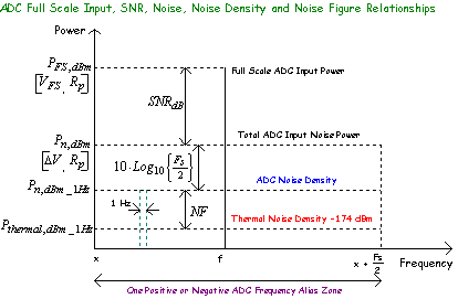
Similar analysis can be applied to DAC’s based on FS, SNR, and Noise Density. Current DAC’s tend to be somewhat more non linear than ADC’s and will exhibit a number of discrete output signals that may be much greater than expected from their Bit resolution. If a sinusoidal signal is generated, this non-linearity will result in harmonics at multiples of the sinusoidal frequency. These harmonics will then enter higher Nyquist frequency zones and “fold back” into the wanted 1st positive alias zone. It should be noted that DAC’s, unlike ADC’s, use a sample and hold output stage and therefore exhibit a Sinc{x} frequency response. Harmonics reappearing in the wanted first positive alias zone will therefore be attenuated by this Sinc{x} response.
Note: Some recent “Tx DAC” devices (Analog Devices) are designed to also operate in the first negative alias zone. These are intended for IF signal construction, followed by Analog based frequency conversion up to higher frequencies.
Typical RF DAC’s use a constant
current differential output with FS = ±10
mA or less. These may be differentially terminated with a 200 Ohm resistance
intended to drive a 200 Ohm differential load. This results in a voltage swing
of ±1
V into a 200 load, i.e.
![]() .
.
The DAC spurious output energy arises from discrete and random causes. Non-linear mechanisms, such as level dependant output compliance (output impedance variation with voltage) create harmonic energy and folds back into Nyquist zones to create non-harmonically related discrete spurious terms. These are DAC device dependant and improve when balanced outputs are used.
Spurious energy caused by random (quantization
+ dither) processes can be interpreted as equivalent discrete energy based on a
given measurement bandwidth
![]() . The theoretical overall noise based spurious output energy for signals
referenced to FS is therefore
. The theoretical overall noise based spurious output energy for signals
referenced to FS is therefore
![]() …(17)
…(17)
This equation represents a best-case
estimate based on Bit resolution
![]() , Sample rate
, Sample rate
![]() , Measurement Bandwidth
, Measurement Bandwidth
![]() and the actual measurement centre
frequency
and the actual measurement centre
frequency
![]() .
.
For example, consider a low cost 10 Bit DAC sampling at a rate of 50 MHz used for PMR transmitter applications with a measurement bandwidth of 8 kHz. A measurement frequency of 1 MHz would produce a noise based spurious output power ratio of 135.9 dB_1Hz or 96.9 dB total in the measurement bandwidth. This is significantly better than most transmitter spurious output requirements based on discrete spurious output energy. For example, a typical PMR Hand Portable will have a transmit output power of 4 Watts, or +36 dBm, and may need to comply with a spurious output power limit of –36 dBm, i.e. a ratio of 72 dB. In this example, the selected DAC would have an effective noise based spurious output ratio that would be about 25 dB better than required. The Sinc{x} sample and hold process would further improve this ratio at higher offsets, as would the effect of additional anti-alias rejection filters required, for example, on the I and Q DAC’s used in a Cartesian Feedback RF PA linearization topology.
Unlike DAC devices, a pipeline ADC, typically used in RF applications, takes a number of clock cycles during acquisition. This typically ranges from a delay of 5 to 14 clock cycles. In some applications, such as Digital Cartesian RF PA feedback loops, the phase margin erosion caused by “Latency” requires consideration. This Latency, or clock cycle delay, generally increases as Bit resolution increases. A typical 8 Bit 50 MHz ADC will require 5 clock cycles to process an input signal, while a 12 Bit equivalent device may require 12 clock cycles.
The additional ADC phase shift
![]() at frequency
at frequency
![]() caused from a Latency of
caused from a Latency of
![]() clock cycles can be predicted from,
clock cycles can be predicted from,
![]() …(18)
…(18)
As an example, a 12 Bit ADC clocked at 60 MHz with a Latency of 12 clock cycles will introduce a phase shift of 0.628 radians (36 degrees) for an input frequency of 500 kHz. When used in a feedback system, some phase margin loss will occur.
We will use the MAX1193 dual ADC as an example. This device has the following performance parameters
|
Parameter |
Value |
Units |
Comment |
|
Supply Voltage |
2.7 ~ 3.6 |
Volts |
Separate Analogue and Digital (1.8 ~ 3.6 V) Supply, |
|
Supply Current |
24 |
mA |
Clocked at 45 MHz, both ADC’s on |
|
Full Scale Input |
± 0.512 |
Volts |
Differential Input, Value Can Be Changed Externally |
|
Bit Resolution |
8 |
Bits |
|
|
Differential NL |
± 0.16 |
Bits |
Maximum limit is ± 1Bit, i.e. monotonic |
|
Integral NL |
± 0.15 |
Bits |
Maximum limit is ± 1Bit, i.e. monotonic |
|
Typical SNR |
48.5 |
dB |
Theoretical = 49.9 dB, ENB = 7.7 Bits |
|
Maximum Clock Rate |
44 |
MHz |
Current reduces for lower clock rates |
|
Input Resistance |
120 |
KOhm |
Essential infinite |
|
Input Capacitance |
5 |
pF |
-j 707 ohms at 45 MHz – (500 MHz with 20 nH) |
|
-3 dB Bandwidth |
440 |
MHz |
Up to Nyquist zone 10. |
|
Latency |
5 |
Cycles |
Channel A, Channel B is 5.5 cycles |
|
RMS Aperture Jitter |
2 |
ps |
Corresponds to a SNR limit of 65 dB at 45 MHz input |
|
Wake Up Time |
20 |
us |
Excellent for low duty cycle power save modes. |
The MAX1193 ADC is well suited to sub sampling operation due to its high input bandwidth of 440 MHz and relatively low aperture jitter of 2 ps RMS. In fact, this low value of aperture jitter would allow input signal capture up to 299 MHz with less than 3 dB deterioration in SNR. (i.e. SNR = 48.5 dB from this mechanism alone, equal to the specified lower frequency SNR)
We will use an IF input frequency of 45 MHz in this example, and select a clock frequency of 40 MHz. This will result in a Nyquist first positive alias of 45 – 40 = 5 MHz.
We will also need to provide a reference impedance at the ADC input in order to predict overall RF and IF gain requirements. It would not be recommended to attempt matching directly into its high input resistance of 120 kOhm at 45 MHz, as this would require very high Q matching elements and is certain to result in extremely poor linearity. The 5 pF input capacitance will represent a reactance of –j 707 Ohms at 45 MHz, so a value of 500 Ohms would probably be more realistic. We will therefore terminate the ADC input with a 560 Ohm resistor and provide a simple reactive match between this input and the previous IF gain stage.
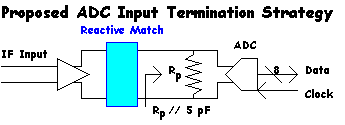
We first need to determine the ADC Noise Figure based on this termination strategy.
|
Parameter |
Value |
Units |
Comment |
|
Full Scale Input |
± 0.512 |
Volts |
Differential Input Peak Voltage |
|
Terminating Resistance |
560 |
Ohms |
In parallel with 120 kOm and 5 pF |
|
Full Scale Input Power |
-6.3 |
dBm |
|
|
Published SNR |
48.5 |
dB |
|
|
ð Input Noise Power |
-54.9 |
dBm |
Spread over one Nyquist + or – alias zone |
|
Clock Frequency |
40 |
MHz |
Results in alias at 5 MHz |
|
ð Input Noise Density |
-127.8 |
dBm/1Hz |
|
|
Themal Noise Density |
-174 |
dBm/1Hz |
Approximate at 25 C |
|
ð ADC Noise Figure |
46.2 |
dB |
Excess noise above thermal noise density |
The combined ADC and termination resistance will exhibit a Noise Figure of 46 dB. This provides some insight into the total IF and RF amplification requirements. For example, if a noiseless gain stage was used with 46 dB of gain, then the ADC input referred noise would be equal to thermal noise and the overall Noise Figure would therefore be 3 dB. A simple rule of thumb is to set the preceding gain equal to the difference between the ADC Noise Figure NFADC and the Noise Figure of the preceding combined amplification stages NFRx. The combined overall Noise Figure will then be 3 dB higher than NFRx. If less amplification is used then the ADC will dominate the overall Noise Figure. If more amplificatiion is used, the overall Noise Figure will improve slightly but ADC overload will occur earlier with increasing signal strength. The 3 dB compromise is therefore an excellent place to start initial system design.
In summary,
![]() …(19)
…(19)
We will assume a combined RF and IF
Noise Figure of
![]() and that a total Noise Figure of 7 dB is acceptable. Equation 19 suggests
and that a total Noise Figure of 7 dB is acceptable. Equation 19 suggests
![]() .
.
We can now begin to make some predictions with respect to sensitivity and dynamic range. A receiver’s sensitivity is usually defined in terms of the input power required to achieve a given demodulated signal quality, usually expressed in terms of SINAD for Analogue FM and BER for Digital modulation Formats. These can be compared (see Appendix),
|
Modulation
Format |
Criteria |
SNR
Required |
IF
Bandwidth |
Sensitivity
@ NF=7dB |
|
Analogue FM NB |
SINAD > 12 dB |
5 dB |
8 kHz |
-120 dBm |
|
Analogue FM WB |
SINAD > 12 dB |
8 dB |
16 kHz |
-120 dBm |
|
APCO 25 4-FSK |
BER < 5 % |
9 dB |
9.6 kHz |
-118 dBm |
|
QPSK |
BER < 0.322 % |
9.5 dB |
20 kHz |
-115 dBm |
|
QAM-16 |
BER < 0.48 % |
16.5 dB |
20 kHz |
-108 dBm |
|
QAM - 64 |
BER < 0.56 % |
22.8 dB |
20 kHz |
-101 dBm |
|
QAM-256 |
BER < 0.60 % |
28.8 dB |
20 kHz |
-95 dBm |
Note: Sensitivity is predicted from
![]()
We will consider the use of Narrow Band FM which will result in a predicted sensitivity of –120 dBm. We also note that the FS input to the ADC was –6.3 dBm and that the preceding combined RF and IF gain was 42 dB. The ADC will therefore reach full scale when the received input signal exceeds –6.3 – 42 = -48.3 dBm. Relative to the predicted sensitivity limit this represents a ratio of 71.7 dB.
A typical low power hand portable receiver might only require a selectivity specification of 60 dB, based on EIA Type Approval compliance limits. The selected ADC would easily achieve this specification with a margin of 11.7 dB. However the equivalent ETS method uses a fixed input on channel level of –107 dBm. In this case the ADC will reach FS when the interfering signals exceed a ratio of 58.7 dB.
It is therefore essential to use a selectable attenuator in the preceeding gain stage, or to extend the selectivity specification by using a xtal filter. Even a wide band Xtal filter can be expected to provide >10 dB adjacent channel attenuation given a narrow band (12.5 kHz) channel offset.
The use of such a filter will extend performance third order intermodulation immunity still further, and will help remove unwanted Nyquist alias responses.
Note: It is always good practise to remove unwanted noise that could fall into other Nyquist alias zones and therefore degrade the ADC Noise Figure performance. Usually a simple LC filter will be adequate. However, the use of a very narrow band filter (e.g. Xtal) directly at the ADC input is not recommended. This may remove beneficial broad band noise within a single Nyquist alias zone and so prevent ADC dither, causing an extreme loss of sensitivity. In ADC devices, noise is actually advantageous.
Analog To Digital Converters process a
given input signal by capturing one sample at a time and translating this into a
discrete digital word representation. The number of quantized steps determines
the “bit resolution” given by
![]() .
.
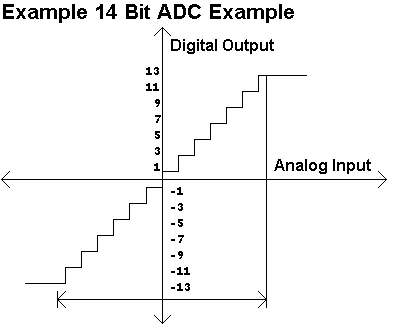
This example ADC has 14 quantized “states” that represent a given input signal. Are these called “14 bits”?
To understand this let us consider the following
0000 = 0
0001 = 1
0010 = 2
0011 = 3
.
.
1110 = 14
1111 = 15 (2^3 + 2^2 + 2^1 +2^0 = 8 + 4 + 2 + 1 = 15)
This 4 bit word can represent numbers from 0 to 15 in integer steps. A 14 Bit ADC can actually quantize input signals into 2^14 states,
14 Bits = 00000000000 to 11111111111111
In other words, the digital output is a
sequence of 14 “o’’s and “1”s that represented the captured input
signal. Therefore a 14 Bit ADC actually has
![]() levels that it can digitally
represent. Let us place this number in perspective
levels that it can digitally
represent. Let us place this number in perspective
ADC Resolution Number of Levels
6 Bit 64
8 Bit 256
10 Bit 1024
12 Bit 4096
14 Bit 16,384
16 Bit 65,536
Our current technology allows designers realistic access to 14 Bit ADC devices that can capture signals at a rate of 100 million times per second. When sub-sampling these devices can represent signals up to 500 MHz, in the digital domain with little loss of resolution.
The Signal To Noise Ratio of an ADC is usually represented as the smallest quantized step relative to Full Scale. In other words we would expect
 …(1)
…(1)
where N represents the number of bits in the digital output word (14 in this example -> SNR = 84 dB). A more accurate analysis will show that this simple formula underestimates SNR by a couple of dB, but this extra theoretical limit of perfection is usually lost in practical devices.
As might be expected, the advent of 14 Bit resolution at 100 MHz sample rates is not a simple little feat. This would correspond to an array of 16.384 comparitors combined with conditional logic to generate a 14 bit output word. This is not something to be wired up on a weekend.
The example 14 Bit ADC with its 84 dB
SNR might seem like an excellent component, but let’s place even this
performance into perspective relative to thermal noise. All ADC devices have a
maximum analog input voltage, usually 1 ~ 2 V peak. Let us assume
![]() , and that the ADC is at the end of a 50 Ohm system. Its maximum input power is
, and that the ADC is at the end of a 50 Ohm system. Its maximum input power is
![]() …(2)
…(2)
This implies
![]() . Given a 84 dB “aperture” resolution, the minimum quantized input power
step would be –74 dBm. Since thermal noise at room temperature is –174
dBm/1Hz, it could be said that the ADC aperture sensitivity was 100 dB larger
than the equivalent thermal noise!
. Given a 84 dB “aperture” resolution, the minimum quantized input power
step would be –74 dBm. Since thermal noise at room temperature is –174
dBm/1Hz, it could be said that the ADC aperture sensitivity was 100 dB larger
than the equivalent thermal noise!
If the ADC devices were really this deaf, we wouldn’t probably want to use them. However a nice trick of nature comes to our rescue.
Imagine, for example you have a stiff and squeaky door. If you try to move it, it will go in small quantized steps. However if you wiggle it back and forth (i.e. “dither it”) then a much finer placement resolution will be possible. A similar effect can be seen in the overall position of a swarm of insects, e.g. bees. Individual animals will flit to and fro in a chaotic manner, but the overall body of insects will appear to be stationary. So although a given transition can appear to be “quantized” some randomising force, even if far greater than the transition step alone, can help “smooth out” the movement and attain much finer resolution. This is how dither operates.
Most high resolution, high speed ADC devices self dither on their own. If dither is required, as might be needed for low speed instrumentation applications, a source of random noise can be injected into the ADC input, and as long as this occupies a spectrum that is different that the measured spectral range, no degradation in sensitivity will result. In fact the actual sensitivity may improved by many decades!
The actual improvement is easy to calculate. If the ADC is under some random process, then its otherwise discrete spurious outputs caused by quantization will be “smeared out” in the frequency domain. The total discrete energy will in fact be evenly spread from DC to ½ the ADC sample rate. So if we now want to express a dithered ADC SNR in terms of spectral noise density, we have
![]() …(3)
…(3)
Now let’s have another go at that 14 Bit ADC sampling at 100 MHz (57 dB). The effective dithered SNR will be
SNR = 84 + 57 dB = 141 dB/1Hz
Since
![]() , it follows that the effective dithered ADC input noise floor must be –131
dBm/1Hz. Compared to a thermal noise floor of –174 dBm/1Hz, it equally follows
that the dithered ADC in question must have a Noise Figure of NF
= 43 dB.
, it follows that the effective dithered ADC input noise floor must be –131
dBm/1Hz. Compared to a thermal noise floor of –174 dBm/1Hz, it equally follows
that the dithered ADC in question must have a Noise Figure of NF
= 43 dB.
Note, this is far superior to an effective aperture limited sensitivity that was 100 dB above thermal noise. In other words, dither has resulted in a sensitivity improvement of 57 dB.
The high resolution, high speed ADC is now a firmly placed member in the world of RF componentry. Although it produces digital output words, its input is definitely in the analog domain. Even its input clock source is an analog signal, and requires the same treatment with respect to minimising noise as in any RF application, although it may be seen as only be a “0” or “1” transition.
The ADC does however have some unusual
properties. Use advantage can be made from its alias response, as in sub sampled
applications. In this mode, the ADC can capture a much higher frequency than ½
its sample rate, and effectively “fold back” the incoming signal frequency
into a frequency region contained within DC to ½ the sample rate. However the
maximum bandwidth available is still limited to
![]() .
.

Sub sampling applications require a Band Pass Filter to be placed in front of the ADC to reject unwanted alias zones. The highest alias zone that can be used is limited by the width of the sample and hold sample that is captured by the ADC, i.e.
![]() …(4)
…(4)
where
![]() represents the width of the
captured signal. For example, a typical 40 MHz sampling ADC can capture signals
up to 350 MHz with little performance degradation. However the quality of the
clock is important, as any phase noise or jitter is multiplied up by the
effective alias ratio. Also, the negative alias responses will have an inverted
frequency spectrum compared to the positive alias response.
represents the width of the
captured signal. For example, a typical 40 MHz sampling ADC can capture signals
up to 350 MHz with little performance degradation. However the quality of the
clock is important, as any phase noise or jitter is multiplied up by the
effective alias ratio. Also, the negative alias responses will have an inverted
frequency spectrum compared to the positive alias response.
The use of the alias response allows good system performance without the excessive current consumption that might otherwise be required for over-sampled cases. For example, a 40 MHz sampling ADC can readily process a 130 MHz IF signal, and produce the equivalent of a 10 MHz digital output word. In this case a special relationship of sample rate relative to output rate exists. By using a sample rate (or alias) that is four times the required output rate, then any subsequent LO used for Digital IF to IQ conversion, can be represented as a sequence of integer +1, 0, -1 values, in other words 4 samples on a sine or cosine wave. This can reduce computational effort by avoiding the need for real by real multipliers and sine – cosine look up tables.
As mentioned before, the high resolution, high speed self dithered ADC behaves as an equivalent “perfect” converter with additional input noise applied as predicted from its equivalent Noise Figure. This equivalent Noise Figure is given by
![]() …(5)
…(5)
where Vpeak represents the maximum ADC input voltage for Full Scale operation, Rp represents the equivalent parallel resistance that is presented to the ADC input, N is the number of bits and Fs is the ADC sampling rate.
Let us assume the following example
Rp
= 50 Ohms
Vpeak
= 0.5 V
N
= 12 Bits
Fs
= 65 MHz
Equation 5 predicts NF = 29.1 dB.
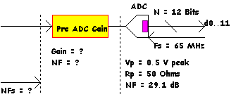
So how do we determine how much gain to stick in front of the ADC? Here is a simple method to start with. Let’s say we want an overall system Noise Figure of NFs = 7 dB, say. If the ADC has a NF of 29.1 dB, and we slap a noiseless amplifier in front with a gain of 29.1 – 7 = 22.1 dB, then the composite result would have a noise figure of NFs = 7 dB. However finding that golden noiseless amplifier can be a bit of a bind, and perhaps a real amplifier might only have a NF of 4 dB (MMIC typical result). So lets add 3 dB to the gain, i.e. 25.1 dB. Where it for the ADC noise alone, the new composite noise figure would be 29.1 – 25.1 dB = 4 dB, the same as the RF amplifier noise!. The noise of the amplifier will be uncorrelated to that of the amplifier, so the 4 dB of the amplifier will add 3 dB to the projected 4 dB of the ADC contribution, giving and overall system noise figure of NFs = 7 dB.
A good starting compromise in any pre-ADC gain stage(s) is to set
![]() …(6)
…(6)
Whether this gain is single frequency or the result of multiple frequency conversions is neither here nor there. The overall pre-gain block will achieve the best compromise between sensitivity and potential signal overload if equation (6) is followed. Adding additional gain will then claw back as much as 3 dB potential sensitivity, but ADC overload will be immediately possible. Applying less gain will reduce sensitivity, by available dynamic range may not substantially improve.
High resolution high speed RF ADC devices usually capture input samples and transfer this information into charge stored on a capacitor prior to digitisation. As might be expected, a “sloppy” source impedance might reduce the accuracy of this process. More fundamentally, the ADC input can be represented as a “1 port” non linearity, and its signal level dependant non linearity can introduce additional distortion to finite source impedance input signals.
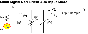
The effect of the variable ADC input impedance over its input signal trajectory can be viewed as an equivalent distortion related current injected in parallel with its input, caused by this non linearity. The resulting non linear voltage components will therefore be proportional to the total parallel impedance the ADC input “sees”.
For example, a given 12 Bit ADC may be presented as having an input inmpedance of 250 Ohms (AD9042), but if it is matched to this impedance using a 50 Ohms source, its linearity will be poor. Best 3rd order intermodulation performance will occur if it “sees” an imnpedance less than 50 Ohms. For this reason, it is often a good idea to immediately define the ADC input impedance with a parallel resistor selected to result in a 50 Ohm input (convenient also for test purposes). This, combined with the source impedance (50 Ohms) will result in an overall source impedance of 25 Ohms at the ADC input.
Given that these analog imperfections have been side stepped by selecting a low source impedance, the 3rd order intermodulation performance of the ADC can now be interpreted. Bear in mind though that the ADC IP3 Figure of Merit (FOM) is best used for comparison purposes with associated RF components, as it non linear behaviour is fundamentally different.
For traditional RF components components we typically find that a 3rd order intercept point predicted from
![]() …(7)
…(7)
represents a useful device or system measurement. This equation assumes that 3rd order product amplitudes increase 3 dB for each 1 dB increase in a corresponding 2 – tone input signal. ADC’s devices however do not naturally exhibit this behaviour – instead their intermodulation products lay smeared out over their input noise figure for any input amplitude below Full Scale (FS).
We will define an “upper limit” to ADC IP3_in given by
![]() …(8)
…(8)
EXAMPLE:
Vp = 0.5 Vpeak, Rp = 50 Ohms, N = 12 Bit Resolution, Fs = 65 MHz, BW = 8 kHz
ð
![]()
Note the –6 dB terms refers to the need to back off each of the two input signal generators by 6 dB so as not to exceed the Full Scale input range of the ADC.
Compared to its analog RF counterparts, this represents a very high IP3 indeed. Even ultra low distortion low noise high speed Op-Amps will not meet such a challenge. A typical MMIC driver, for example, might only have a corresponding output 3rd order intercept point of +40 dBm, and require 75 mA of supply current (e.g. SGA-6489). A corresponding high performance Op-Amp will seldom exceed an output intermodulation ratio of 80 dB, so at 0.5 V output, these devices will have a similar IP3_out as the MMIC, but achieve the result at a lower supply current. However their class AB output stage is their prime limitation, and when asked to provide 20 dB of RF gain (as opposed to unity gain), they will become substantially less linear.
This Digital Variable Gain Amplifier (DVGA) amplifier from MAXIM-IC represents the latest state of the art in IF-ADC interface technology

and is a good complement to the

dual ADC from Analog Devices
The previous IP3 analysis might promote an overly rosy future for the good ol’ ADC. Although the device offerings of today are too far off the mark, the deterministic non linearities can be a “shoe horn” into unexpected spurious response anomalies.
Recall that the ADC has a multitude of potential alias conversion mechanisms, and any harmonics generated from internal or external non linear mechanisms can evoke an unwelcome response.
For example, let us assume an application in which a total RF input frequency range of 550 kHz to 30 MHz is to be digitally converted by an ADC. Let us assume a 14 Bit ADC sampling at 65 MHz, just high enough to allow the first negative alias response above 35 MHz to be rejected. However spurious response mechanisms at 1/2 , 1/3 f are possible, but even more insidious are the following,
RF = 25 MHz, Harmonics at 50 MHz, 75 MHz, 100 MHz, etc
F Sample = 65 MHz
25 MHz is represented correctly as a 1st positive alias of Fs=65 MHz of f = 25 MHz
75 MHz is represented as a 2nd positive alias at +10 MHz output (75 – 65*1)
100 MHz is represented as a 2nd negative alias at –30 MHz (65*2 – 100 = 30 MHz)
etc. These spurious responses can only be prevented if attention to linearity is paramount. We will adopt the definition of following alias zones

These self induced non linearity response zones are predictable, and are best managed by ensuring that preceding non linearity’s in subsequent RF amplifying systems do not contribute significantly to the fundamental quantized-dither limited ADC performance. Also the ADC one port non linear behaviour can be easily offset by the application of a low source impedance. Being an RF component, impedance values around 50 Ohms are quite appropriate.
As previously mentioned a typical RF oriented ADC will have a potential input bandwidth that will far exceed their 1st positive alias zone. It is important that any preceding amplifying stages do not introduce unnecessary noise into these zones. For example, let us consider a 50 MHz sampling ADC with a –3 dB input bandwidth of 500 MHz. This device will be capable of “interpreting” an input signal over at least 20 alias zones. The effective noise contribution could be 13 dB higher if some band pass filtering is not included.
There is a corollary to this however – lower resolution ADC devices may not “self dither” and if too narrow a band-pass filter is used, the preceding amplifying devices may not be able to introduce sufficient noise to ensure that at least one bit is always toggling. Typical high speed RF devices tend to fall into the following categories
6 Bit Can sample > 2 GHz Often Low Cost
8 Bit Very common low cost (MAXIM-IC ~ $2), available up to 40 MHz
10 Bit Same as above but more expensive ($5~10)
12
Bit Classic AD9042 40 MHz RF ADC
Many variants ~ $15
14 Bit Best RF ADC technology available to date
16 to 24 Bit – Audio, sigma delta, low frequency < 1 MHz only
RF ADC devices can achieve superb performance and the advent of 14 Bit devices that sample up to 65 MHz represents a significant human achievement in mixed signal device technology.
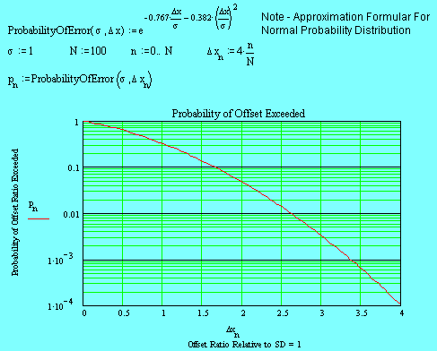
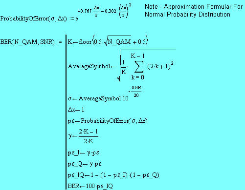
This model is based on a Normal
Distribution associated with a random noise vector that causes symbol decision
errors dependant on the noise vector’s amplitude standard deviation
![]() and the decision threshold
and the decision threshold
![]() .
.
The noise vector standard deviation
![]() is directly related to the I or Q
channel noise power and the “Average Symbol Power” as follows,
is directly related to the I or Q
channel noise power and the “Average Symbol Power” as follows,

For example, QAM64 has 8 Symbol Levels for channel I, and 8 Symbol Levels for channel Q. The product results in 8 * 8 = 64 combinations, hence QAM64.
It is convenient to think of each level in terms of ±1, ±3, ±5 etc. Consequently, the possible “energy levels” are 1, 9, 25 etc. Since each symbol energy level is equally probable, the average symbol energy is simply an average over all energies.
Given this definition, the decision threshold is ±1, since the distant between adjacent symbols is 2.

Consequently, if we know the standard
deviation of the noise term
![]() , then we can determine the probability that the symbol value will be estimated
in error. This standard deviation is,
, then we can determine the probability that the symbol value will be estimated
in error. This standard deviation is,
![]()


![]()
Return to: A Component Universe
or: Ian Scotts Technology Pages
© Ian R Scott 2007 - 2008