or return to Curious Mathematics
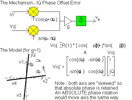
Analog IQ modulators (and demodulators) have enjoyed a recent technology boost in linearity and broad band noise. However they contain imperfections describe by IQ DC offsets, IQ gain imbalance and IQ phase skew errors. These mechanisms contribute an ultimate in band Signal to Noise Ratio (SNR) between 30 to 40 dB.
However, these errors can be easily estimated and corrected, although this is not well realized. We begin with a simple model,
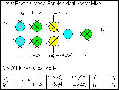
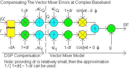
The IQ modulator, with imperfections, is considered as a "perfect" IQ modulator with imperfection terms added at its input. IQ DC offsets, leading to carrier leakage are simple additive terms, gain imbalance is a simple scaler multiply term and phase skew errors are represented by a matrix - note the signs involved as this is not a rotation matrix.
We may want to estimate these errors and remove them. It is easy.
The following syntax will be adopted
![]() - kth detected RF voltage (e.g.
small letters from diode detector)
- kth detected RF voltage (e.g.
small letters from diode detector)
![]() k-th Complex Baseband signal
voltage (i.e. LARGE letters - from FPGA/DSP)
k-th Complex Baseband signal
voltage (i.e. LARGE letters - from FPGA/DSP)
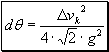
![]() - a difference between the square
of 2 detected RF signals
- a difference between the square
of 2 detected RF signals
The errors incorporated in the model are considered to be small compared to actual signal magnitudes. As a result high order error terms will be discarded when convenient.
A family of 8 DC test vectors will be adopted
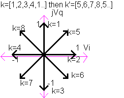
This corresponds to "off line training" - I will discuss how to do on line training later.
This enumeration strategy allows a convenient k and k+1 vector label between successive data points. Two vectors are required to extract each parameter, but groups of estimates can be averaged to reduce possible estimate bias.
Once all 8 test vectors have been sent, and 8 DC RF voltages have been collected, the algorithm will interpret the IQ error parameters and apply compensation. This process will be repeated until adequate system performance is obtained.
Although 8 DC test vectors are suggested, it may be possible to work with a reduced set. In principle 2 vectors, i.e. 2 I and 2 Q signals should be capable of estimating 4 DC error parameters, but may produce bias. A compromise set of 4 DC vectors will also be proposed, corresponding to k=[5,6,7,8,5].
2.
Mathematical Analysis
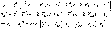
The effect of DC IQ offset will be considered first, followed by amplitude imbalance and non-quadrature phase imbalance. In addition, a method for compensating the relative phase between up and down IQ conversion processes within the Cartesian feedback system will be discussed.
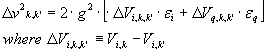
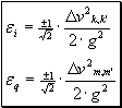
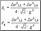
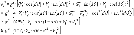
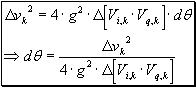
In both cases a model based parameter extraction process will be applied. This will be staged as 3 independent estimates arising from 4 independant mechanisms of DC I offset, DC Q offset, relative IQ gain and non quadrature IQ phase error. (i.e. we assume that an error in DC offset, for example, should have a minor effect on other estimates). It is expected that this assumption will not be completely valid, and the convergence path may not be simple. The solution is to adopt an iterative procedure based on advancing the direction of a solution in the most favorable direction. For each parameter we will produce updates given by
![]()
In this way the requirement for “estimate independence” is relaxed, and convergence can always be ensured with a suitable value for “stepsize” (e.g. ~0.5-0.9) used to update values for each parameter.
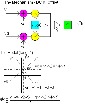
Assume
![]()
and
![]()
where
![]() ...(1)
...(1)
to represent the effect of a small IQ DC offset. This systematic error will cause predictable envelope variations between the suggested DC test vectors, which can be monitored using a simple diode detector placed in the RF path.
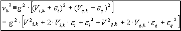
The
detected RF envelope voltage
![]() for a k-th test vector can be represented as
for a k-th test vector can be represented as
![]() …(2)
…(2)
Here g represents the IQ to DC conversion gain of the system. When IQ DC offset is introduced, the new predicted RF envelopes become
![]() ...(3)
...(3)
Squaring both sides provides,
 ...(4)
The trick now is to select candidate DC test vectors for the I and Q
channels that allow a cancellation of terms. In this example we will select 2
Complex Baseband test vectors (k and k’) that satisfy
![]() and
and
![]() . (i.e. these cancel but the
linear terms add)
. (i.e. these cancel but the
linear terms add)
The variation in the detected RF power (voltage squared)
![]() between these 2 test vectors is
between these 2 test vectors is
Considering the case where
![]() we have,
we have,
 …(5)
…(5)
Consequently the predicted IQ DC offset errors are,
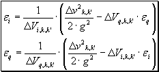 …(6)
…(6)
providing the
denominator terms do not equal 0 for a given test vector pair. The trick now
is to “uncouple” the error term estimates by setting
![]() but
but
![]() for the I channel error estimate,
and
for the I channel error estimate,
and
![]() but
but
![]() for the Q channel error estimate (note – these are both real
unlike
for the Q channel error estimate (note – these are both real
unlike
![]() which is complex).
The previously indicated DC test vectors are proposed,
which is complex).
The previously indicated DC test vectors are proposed,
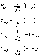 …(7) swap
3 - 4
…(7) swap
3 - 4
These test vectors have unit magnitude with 4 phases. The actual differences between groups of 2 vectors k and k’ at Complex Baseband will now be,
 …(8) note
- +j0 i,q
…(8) note
- +j0 i,q
with indice notation 1,3 used to suggest vector 1 minus vector 3, as shown in equation (5).
Equation (6) can now be simplified,
 ...(9a)
I and Q DC offset errors can now be determined from each pair of test vectors. With four test vectors, 2 estimates for each error can be determined, and averaged to improve accuracy. With the given vectors, k,k’ = [1,3] and [2,4], while m,m’=[1,2] and [3,4]
 …(9b) update indices
note: small v is used to represent detected RF voltage.
The intention is to reduce potential bias in the estimates for IQ DC offset parameters. (i.e. the result should be relatively independent of other system errors.)
Worked
Example
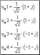
Let ei = 0.1, eq = -0.2 and g=1. For test vectors 1 and 2 we have
Viq1 = (0.707+0.1)
+j (0.707-0.2)
Viq2 = (0.707+0.1)
+j (-0.707-0.2)
The detected voltage squared (Vi^2+Vq^2) is now
v1^2 = 0.908
v2^2 = 1.474
The difference is -0.566 volts squared. In this example the same result will be obtained with vectors 3 and 4. Substituting into equation (9) correctly predicts eq = 0.2001.
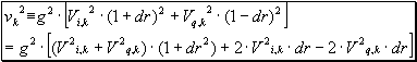
2.2.
IQ Relative Amplitude Offset Compensation
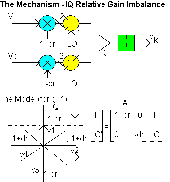
The relative IQ gain offset is represented as dr, and the absolute gain as g. The absolute gain g can be computed prior to the extraction of other parameters (simply an average of 8 measured RF DC voltages if a test vector magnitude of “1” is assumed ). This initial procedure may help assist convergence later on, especially if g is larger than expected.
In this case we want to infer the relative amplitude skew parameter “dr” from envelope information, given that we can again propose suitable DC IQ test vectors.
 …(10)
…(10)
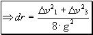
Let us take 2 vectors k and k’=k+1 from our test family and look at the difference in the measured RF envelope,
If we assume a maximum gain imbalance of 1 dB (say), then dr ~ 0.05. (i.e. +/- 0.05 = 0.1). The dr^2 term is therefore relatively insignificant and will be ignored. The relative difference between two vectors k and k’=k+1 is then,
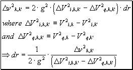 ...(11)
Let us now define 2 “appropriate” test vectors,
 ...(12) note
- i.e. not
the square of the difference!
...(12) note
- i.e. not
the square of the difference!
Since the difference is 2, equation 11 simplifies to,
 ...(13)
If we want to use “45” degree vectors, these become,
 ...(13a)
with a modified result that,
![]() ...(13b)
...(13b)
Consequently this proposed set is not appropriate.
Continuing with the previous vector set... For good measure 2 additional test vectors will be added,
 ...(14)
which allows 2 estimates for dr, leading to a (better) average estimate of,
 ...(15)
Worked
Example;
Let dr=0.1 and g=1. Test
vectors 1 and 2 imply that the change in detected voltage squared will be (1.1^2
+ 0^2) - (0 + 0.9^2) = 0.4 V^2. Substituting
![]() into equation (13) immediately
predicts the gain offset of dr=0.1.
into equation (13) immediately
predicts the gain offset of dr=0.1.
2.3. IQ Non Quadrature Phase Offset Compensation
This mechanism is the result on non quadrature phase error inside the LO quadrature splitter of the Vector Mixer. As a result, it will be interpreted as a relative phase error, as opposed to an absolute phase error.
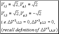
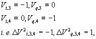
This error mechanism causes a clockwise rotation of the Q channel and a counter clockwise rotation of the I channel for a positive phase error (i.e. not a simple rotation in absolute phase). To show this let I=cos(theta), Q=sin(theta) and expand the terms,
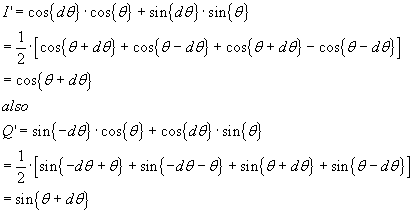
 ...(16)
We will use test vectors that satisfy
![]() and
and
![]() and consider the difference
between 2 such vectors in equation (16),
and consider the difference
between 2 such vectors in equation (16),
 ...(17)
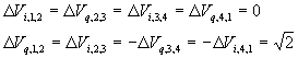
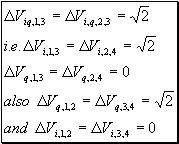
In the case the previous 4 vector pair used for IQ DC imbalance estimation are suitable, i.e.
 ...(18)
Test vectors 1 (IQ_product =
![]() ) and 2 (IQ_product=
) and 2 (IQ_product=
![]() => difference is
=> difference is
![]() ) can provide one phase estimate in (17) and test vectors 4 (IQ_product =
) can provide one phase estimate in (17) and test vectors 4 (IQ_product =
![]() ) and 3 (
) and 3 (
![]() *IQ_product =
*IQ_product =
![]() => difference is
=> difference is
![]()
![]() ) can provide a second estimate. In this case equation (17) becomes,
) can provide a second estimate. In this case equation (17) becomes,
 ...(19) -
It is suggested that the IQ training vectors be applied off line, after which the solution should remain relatively stable for a period of minutes to hours. One suggested sequence is
1.
Apply DC offset correction vector set and record results
2.
Calculate absolute Viq to v gain “g”
3.
Calculate IQ errors i.e. DC offset, gain imbalance and phase imbalance
4.
Update each parameter by
![]()
for
iteration m+1
5.
Apply parameter set at complex baseband to remove errors
6.
Return to 1 and repeat until a minimum error is obtained
Since the parameters are model derived (as opposed to a random search), convergence should be fast, and errors will reduce by a large ratio per iteration. As a result, only 10 iterations may be necessary. If the loop settling time is 20 uS (say), then the job may finish in 8*200 uS = 1.6 mS.
Once this DC training is done, the transmitter can be returned on line and the relative LO phase can be updated from time to time as a background task.
visit a circuit compensator? Hardware Compensation Circuit
return to Curious Mathematics
or home page Kaleidoscope Comms