


![]()
This document opens with a short history on diode applications in general, beginning with the primitive “almost a diode” Coherer detector used for Morse Code reception and rusty copper oxide AC-DC rectifiers. Better semiconductor materials such as Selenium were soon discovered, leading to higher voltage AC to DC power rectification and low frequency audio signal application. RF signal applications began around the time of the “point contact signal diode”, which had sufficiently low capacitance to allow signal detection up to several hundred MHz. Germanium gained an early status due to its ease of manufacture and today Silicon reigns. Much interest is also shown in Carbon (diamond) and compound semiconductor materials such as Gallium Arsenide, Silicon Germanium, Indium Gallium Phosphorous, etc.
This document describes the construction and characteristics of the following diode classes.
| Early
Semiconductor Diode (or Diode Like) Devices |
-
The
“Coherer” used to receive slow speed Morse code radio messages
-
The
Copper Oxide “Battery Charger” Rectifier
-
The
Higher Voltage “Selenium” Rectifier
-
The
Small Signal Audio Diode, Also Based on Selenium
-
The
First RF Component, The Germanium Point Contact Signal Diode
| More
Recent Semiconductor Diodes |
-
The
Germanium PN-Junction Diode Used For Switching
-
The
Tunnel Diode (Or Esaki Diode after its Inventor Leo Esaki)
| Modern
Semiconductor P-N and Related Junction Diodes |
-
The
Silicon Diode Used For Switching
-
The
Schottky Diode Used For High Speed Rectification and Microwave Applications
-
Silicon
and Gallium Arsenide Variable Capacitance “Varactor” or “Varicap” Diodes
Used For Electronic Tuning in Filters and Oscillators
-
Silicon
Zener and Avalanche Diodes Used For Voltage Regulation and Clamping
-
Silicon
P-I-N Diodes Use For Variable Attenuation and Band Switching
-
Photo-Detector
Diodes
-
Solar
Cell Diodes
-
Light
Emitting Diodes (LED’s and also LASER Diode)
The electrical characteristics for the following topics are also described in further detail.
·
PN-Junction
Diode Static V-I Characteristic
| Reverse
Biased Varicap Diode C-V Characteristics | |
| PIN
Diode Carrier Lifetime
| |
| Forward
Biased PN-Junction Diode “Charge Based” Capacitance |
The semiconductor age has revolutionised electronics with miniaturised circuits performing convenient, advanced signal processing functions. Semiconductor devices are used for power electronics, audio amplification, radio frequency amplification, optical processing and digital computations.
Prior to this we lived in a land of
wires, relays, twine and sealing wax. Even the emergence of De Forest’s vacuum
tube
 belonged to an era of hand-connected components mounted on bent, drilled and
machined metal chassis bolted into equally hand crafted wooded cabinets.
Although nostalgic to some, individual production of such expensive items was
never an ambition of the industrial revolution. Mass production, based on
repetitive tasks, each being a sub component of the whole, was the enviable
position to be attained. Towards this end we saw the use of PCB substrates
supporting leaded components and socket held valves, each searing their
surroundings with heat for the purpose of relatively simple signal processing.
belonged to an era of hand-connected components mounted on bent, drilled and
machined metal chassis bolted into equally hand crafted wooded cabinets.
Although nostalgic to some, individual production of such expensive items was
never an ambition of the industrial revolution. Mass production, based on
repetitive tasks, each being a sub component of the whole, was the enviable
position to be attained. Towards this end we saw the use of PCB substrates
supporting leaded components and socket held valves, each searing their
surroundings with heat for the purpose of relatively simple signal processing.
The semiconductor promise was one of reduced size and heat, both of which beckoned more complex signal processing tasks to be performed. As the number of semiconductor components increased, reliability issues became increasingly important. Anecdotal stories of house sized computers built with vacuum tubes serviced by teams of technicians repairing defects every few hours are easily found. The translation to transistors, at first based on at least one occasion by the “point contact” germanium transistor improved this situation considerably. The grand centre stage show belongs to the invention of the integrated circuit, for which the photographic process used for device definition and interconnection has become tuned to a fine art. Resolutions available today parade themselves at a fraction of the wavelength of light used for creating the lithographic screens used for device fabrication. Complexity, Heat and Reliability issues are now replaced by those associated with Software Reliability.
The ocean going ships of the time had crude communication technologies, involving the use of semaphore for transferring simple messages, or the use of loud fog-horn calls to at least state occupancy in fog laden seas. In isolation, Nikola Tesla had been experimenting with coils that made high voltage discharges, with a dream in mind of sending electronic power between the continents of the world, huddled between the blankets of transmission line effects between the planets surface and its ionosphere. Equally remote, Marconi also played with sparks, sending them from the ends of one wire loop into the gap of another. In some “lair of Frankenstein” way both experiments sparked forth the birth of a new communications industry. However, the distances electric fields could cross only existed within the confines of a small experimenter’s room. For sea-to-land communications, something more sensitive than the electrical breakdown of air was needed. However, on the positive side (no pun intended), ocean going ships with their massive diesel generators had almost unlimited power to send.
I guess some people thought about this and reasoned that the distance of the receiving spark gap was the other part of the problem. (Perhaps there are transactions on this subject?) How could the gap be made smaller so that the tiny sparks could fly across and make their mark?
One idea was to fill a glass tube with rusting iron filings. Electrodes were attached to each end, and a source of voltage was applied through headphones. Normally the iron filings would make poor contact, but when a RF pulse came along some of the filings would arc and short, allowing a DC current to pass.
|
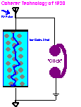
Morse Code was the coherer’s domain and it was firmly thought to be there to stay. Or so it seemed – until De Forest’s vacuum diode came along, and the coherer’s brief life was over.
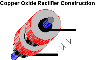
The semiconductor based rectification properties of various metal oxides had been observed long before the invention of the vacuum tube diode. Of these, rectifiers formed from copper disks sandwiched between iron ones were popular. Their main application was for low frequency AC to DC conversion, such as that required for car battery charging. However these assemblies had a relatively low reverse breakdown voltage and several disks were needed to rectify AC voltages even as low as 6 V AC. The unfortunate consequence was relatively inefficient AC to DC conversion efficiency due to the cumulative forward voltage drop of each individual rectifying disk. In addition, the screwed down washer-by-washer construction was not suited to automated construction, although the cost of each iron washer and insulating disc was low.
Selenium rectifiers followed copper oxide devices, and were best suited to lower current, high voltage rectification such as required by valve high tension DC supplies up to 250 V DC. They were also based on a stacked construction, but thin rectangular slabs were used instead of washers. Some small signal “selenium diodes” were also produced, used for audio clipping applications such as car AM radio impulse noise blanker applications.
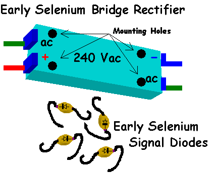
Selenium rectifiers survived for some time as high voltage rectifiers in valve based AM radios for medium and short wave broadcast radios, based on their relatively small size compared to a dedicated rectifier tube, absence of a heated cathode and relatively low cost. Germanium rectifiers were possible at the time, based on alloy junction construction, but had high leakage current, especially with the temperatures expected in a typical valve radio. The high voltages encountered were also a major stumbling block, as the several hundreds of volts required in vacuum tube radios was far high than the 30 V average best ratings of Germanium. Even if these obstacles were overcome, device failure due to “thermal runaway” was probable. Leakage current made worse by increasing temperature lead to additional heating that further exacerbated the leakage problem. Device destruction soon followed. Given this, even stacked series combinations of Germanium diodes were never feasible.
Consequently, Selenium rectifiers lasted right up to the advent of Silicon junction diodes, coinciding about the time of the “planar” photolithographic process. These new improved Silicon devices sprang into the spotlight immediately, armed with forward voltage drops less than 1 Volt and reverse blocking capability exceeding 400 Volts, even to 100 Volts with minor tweaks. Overnight, once again, old technology was tossed out from its comfortable home in favour of the new, and the selenium rectifier’s days of notoriety were over even faster than it ousted the copper oxide rectifier that previously overthrew the vacuum valve.
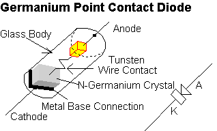
Point contact diodes can be formed by pressure contact between a metal electrode and a semi-conductive substance. The earliest signal detection applications might have involved “Paul Hogan” and his captured men fingering a piece of coal at “Stalag 9” in a TV episode of “Hogan’s Hero’s”, or so when young we might have believed. Such episodes often portrayed a captured soldier straining to hear an allied radio broadcast on a pair of army issue magnetic headphones, right under the nose of the imprisoning “Colonel Clink”. A lump of coal, in this case poised against the spring of a wire whisker, would have contained traces of selenium and containing carbon, was adequately conductive as a substrate. Hence the first “TV Radio Diode!” bought AM (short-wave?) messages to the troops.
Commercial production of point contact diodes began early, fuelled by the communication needs of WW1, but also because they were easy to manufacture, and with profit, also their low self-capacitance made them useful for Radar detection. The standard semiconductor was Germanium.
 |
|
Germanium point contact diodes had reverse leakage currents in the order of 1 uA, and a forward voltage drop around 0.2 V at currents less than 1 mA. They were well suited to RF signal detection at frequencies up to several hundred MHz even in their commercial cylindrical glass package, due to their low self-capacitance usually less than 0.5 pF.
The PN junction was formed from impurities in the wire contact (Tungsten, etc) combining with the Germanium crystal. This was often assisted by “forming”, a process whereby a short electronic pulse was passed between the electrodes. This helped to establish a secure and stable PN region.
Note: In this way the Germanium point contact diode does not resemble a “Schottky” diode, which is based on a direct metal to semiconductor junction. Although a Germanium point contact diode may use a metal contact, this contact is used to form a P-N junction immediately under its tip, and the metal wire contact then becomes a simple connecting electrode.
Although the Germanium point contact diode enjoyed great success as a small signal detection diode, it had a relatively high series resistance that limited its ability to handle currents beyond a few milli-amperes or to act as logic elements in semiconductor based computers. The small area of contact was responsible. In addition, its electrical characteristics were unpredictable, partly due to the mechanical nature of its formulation, the imprecise nature of “forming” and also the uncontrolled impurities that could be expected from one Germanium crystal to the next.
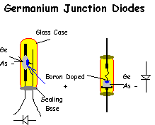
The Germanium junction diode was born from advances in the science of growing large, chemically pure crystals. Further, the concept of “doping” a given crystal with impurities that could result in an excess of electrons (Arsenic doping produces N - Type material) or an excess of holes (Boron doping produces P- Type material) was in hand during the second-world war. Chemical vapour deposition could then be used to create an accurate PN junction on a single Germanium wafer, which could then be bonded to or pressed against suitable wire electrodes.
 |
|
Germanium semiconductor junction diodes reigned up to the 1970’s, used mainly in discrete semiconductor based computer mainframe equipment. They formed simple AND gates and OR gate logic elements that required a low forward voltage drop, fast switching and acceptably low leakage. Once again, however, the tides were turning on yet another established technology in favour of a newer breed. Silicon had long been envied for its high temperature resilience, up to a predicted maximum of 200 C, compared to Germanium that failed miserably at 90 C. Although plentiful (as Silicon-Oxide or sand), purity was a serious barrier to Silicon’s commercial use. Small molecular imperfections could render an otherwise viable PN-Diode structure useless, resulting in unattractively low yields.
The Silicon Junction diode was placed “centre stage” as soon as this crystal purity barrier was broken. These diodes soon adopted the “planar” photographically processed substrate method, and were initially housed in the same glass envelop as their Germanium cousins. They offered a low cost, ultra low reverse leakage diode with excellent RF and switching characteristics. They even replaced the familiar Germanium point contact diode in AM radio detector circuits, especially when these also switched to silicon planar transistors instead of slower, low gain and temperature intolerant Germanium devices.
Today’s Silicon junction diodes are constructed simply without te potentially unreliable wire contact (“whiskerless diode”) and have changed very little from their introduction around 1960. A planar lithographic process is used, and surface mount housing is now standard unless high power dissipation is required.
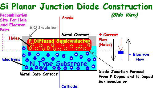
The Silicon (Si) junction diode consists of a N-Type substrate with a Diffused P-Type upper surface. Metal contacts are made to each surface for electrical connection. Potential “Intrinsic” semiconductors and their potential “Doping” elements can be seen as adjacent columns in the following periodic table,
Truncated
Periodic Table
|
Period |
III-A 3-A |
IV-A 4-A |
V-A 5-A |
Advantages
of IVA Semiconductor |
Use |
|
Row |
|||||
|
2 |
B
Boron |
C Carbon |
N
Nitrogen |
Very-High Temperature |
Future |
|
3 |
Al
Aluminium |
Si Silicon |
P
Phosphorous |
High Temperature, Cheap |
Common |
|
4 |
Ga
Gallium |
Ge Germanium |
As
Arsenic |
Now used as SiGe Hybrid, best frequency performance |
Obsolete By itself |
|
5 |
In
Indium |
Sn Tin |
Sb
Antimony |
Sb used for infrared detect |
TBD |
|
6 |
Ti
Titanium |
Pb Lead |
Bi
Bismuth |
(Galena=PbS
+ cats-whisker) |
X-Shield |
|
Donor |
P-Type |
Intrinsic
Semi |
N-Type |
|
|
The P-N junction requires a chemical bond to be formed, usually by heated diffusion of a donor into the intrinsic semiconductor or semiconductor previously doped with the opposite polarity donor. Although N-Type material has an excess of electrons, it is not electrically charged. P-Type is also electrically neutral. The main carrier of charge in N-Type material is the negatively charged electron, whilst the main charge carrier in P-Type material is the positively charged “hole”,
In the absence of any applied voltage, a “depletion” layer of hole and electron pairs form at the P-N junction, much like opposite sides of soldiers lining up for a battle. Neither can permanently cross the barrier height of the junction on their own, as their energy is much less than the energy height of the P-N junction barrier. They have a finite probability of being on the opposite side at any time, based on the mutual attraction of opposite charges, and also the repelling force of same charge carriers. The average separation of these charges is referred to as the “depletion layer”, since the P-Type semiconductor is depleted of holes in this region, and the N-Type semiconductor is depleted of electrons.
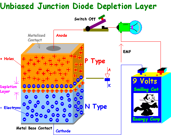
The average density of this “depletion charge” can be shaped by the presence of an external voltage field. Imagine that the positive terminal of a battery is connected to the P-Type Anode, and that the negative terminal is connected to the N-Type Cathode. The positively charged holes will be repelled by the positive charge on the Anode, and be forced down into the depletion region. Likewise, the negatively charged electrons will be repelled by the negative charge on the Anode and be repelled upwards to the depletion region. Electrons and holes will “recombine” in the depletion region, effectively passing through each other much the same way as a drop of rain would pass through an air bubble rising from the ocean.
We will include an indicator Lamp in series to show the effect of current flow.
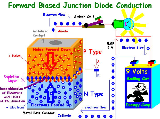
Conversely, if the battery polarity is reversed, the positive holes will be attracted to the now negatively charged Anode and the electrons will be attracted to the positive Cathode. Unlike the previous forward biased condition, in which the depletion layer was squashed together, now the width of the depletion layer increases. No recombination can occur, and therefore a complete current path is not available. Consequently, reverse bias results in blocked current flow.
In practice, conduction is relative. Some current will flow in the reverse direction due to the small presence of holes in N-Type material and electrons in P-Type material. In addition, surface mechanisms for additional leakage may exist. In general, most P-N junctions closely follow a I-V transfer function given by,
![]() …(1)
…(1)
Here
![]() refers to the current flowing from
Anode to Cathode,
refers to the current flowing from
Anode to Cathode,
![]() refers to the voltage from Anode to
Cathode.
refers to the voltage from Anode to
Cathode.
![]() is a “saturation current”
parameter relative to the particular diode (and is temperature dependant) and k
is a constant defined as,
is a “saturation current”
parameter relative to the particular diode (and is temperature dependant) and k
is a constant defined as,
![]() …(2)
…(2)
The constant
![]() represents the electron charge,
represents the electron charge,
![]() is Boltzman’s Constant and
is Boltzman’s Constant and
![]() is an “ideality factor”
depending on the particular diode and semiconductor base.
is an “ideality factor”
depending on the particular diode and semiconductor base.
The PN-Junction diode can be used for RF rectification up to about 100 MHz but becomes limited in its upper frequency capability due to charge storage time. When electrons and holes “combine” in the depletion time, it takes a finite time before they can “pass through” and separate. This “charge storage” time causes the diode to remain conducting for a short time even when it is reverse biased. Consequently, rectification efficiency becomes impaired, falling to almost zero when the charge storage time equals one half period of the RF signal frequency.
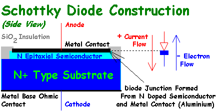
Schottky diodes are usually constructed
as from a Silicon N+ strongly doped material base with a thin N Type Silicon
Epitaxial layer on top. A non-ohmic metal contact is placed on top and this
creates a depletion zone at this junction. The difference in material “work
functions” creates a potential barrier, but in this case only majority
carriers are involved (electrons in both the N Expitaxial layer and the metal
contact). This results in an equivalent “P-N” junction but without the need
for electron-hole recombination. The previous recovery time delay is therefore
avoided, and the turn off time of a Schottky diode is limited only by its
internal capacitance and series resistance. Equivalent values of
![]() are typical for RF Schottky diodes,
compared to
are typical for RF Schottky diodes,
compared to
![]() for small signal junction switching
diodes like the leaded 1N4148 or its SMD BAV99 equivalent.
for small signal junction switching
diodes like the leaded 1N4148 or its SMD BAV99 equivalent.
 |
|
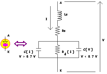
PIN diodes are almost the exact opposite of Schottky diodes in that they seek specifically to have very long charge storage times.
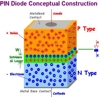
The P-Intrinsic-N or PIN diode has a layer of pure (un-doped) intrinsic Silicon sandwiched between the familiar P and N doped areas. This middle intrinsic layer “traps” hole and electron charges and as a result, the PIN diode takes a relatively long time to turn off, when reverse biased. The amount of trapped charge depends on the current and the volume of the intrinsic layer. Typical recombination times can be in the order of microseconds. As a result, the PIN diode makes a poor rectifier at RF, but can be made into a switch, or a current controlled RF resistor.
Zener diodes and Avalanche diodes have the same basic PN junction structure but operate with completely different physical mechanisms.
All PN diodes are photosensitive to some extent, but different semiconductor materials can modify sensitivity and wavelength specificity.
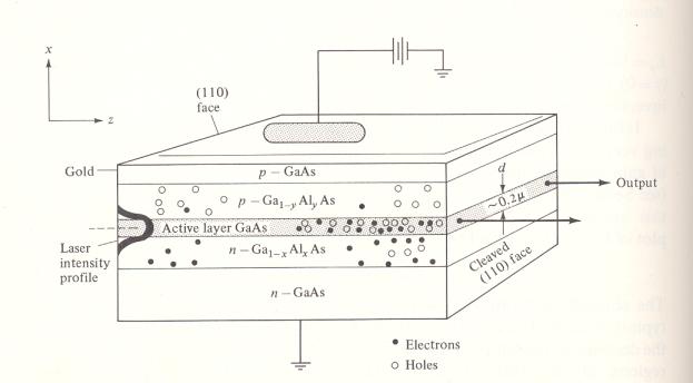
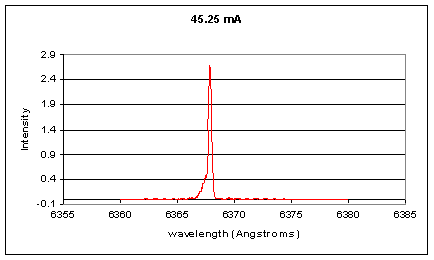
Typical LASER Output Spectrum
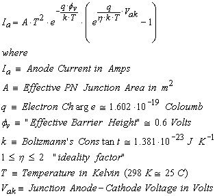
Ideal semiconductor diodes have a voltage dependent Anode current that can be described by the following exponential current versus voltage transfer equation,
 …(1)
…(1)
Equation (1) can accurately describe the
diode’s forward biased electrical behaviour but not the thermal behaviour as
the saturation current term
![]() is strongly temperature dependent.
A more exact model for the diode thermal-electrical behaviour is,
is strongly temperature dependent.
A more exact model for the diode thermal-electrical behaviour is,
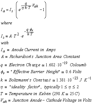 …(2)
…(2)
We will use equation (2) for further junction diode predictions.
Real Diodes have additional series resistance caused by finite conductance in the semiconductor material and ohmic connections made to it.
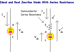
If this total resistance is labelled as
![]() then the real diode voltage can be
expressed as the original forward voltage drop in series with an additional
voltage drop based on current and this added resistance,
then the real diode voltage can be
expressed as the original forward voltage drop in series with an additional
voltage drop based on current and this added resistance,
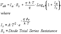 …(3)
…(3)
This diode equation contains a number of coefficients, some of which are fundamental constants and some that are diode dependent.
Real diodes also suffer from additional leakage current paths that become most apparent when operated in reverse bias. This parallel resistance causes additional reverse current. Further, this resistance will be voltage and temperature dependent.
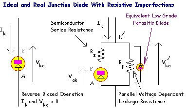
When moderately reverse biased, the
effect of the series resistance term
![]() will be negligible, due to the low
expected current flow. We will propose the following diode model intended for
best accuracy in the reverse biased region,
will be negligible, due to the low
expected current flow. We will propose the following diode model intended for
best accuracy in the reverse biased region,
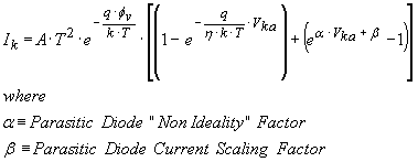 …(4)
…(4)
Equation (4) describes the voltage dependent leakage current that is typically observed in Junction diodes. This behaves similarly to the forward biased characteristic, but has a much higher “threshold” voltage. The second added exponential term accounts for the current contribution from this unwanted “parasitic” diode.
Note:
The current and voltage terms
![]() have been reversed so as to become
positive quantities.
have been reversed so as to become
positive quantities.
All insulating and semiconductor
materials have a certain maximum electrical field strength they can sustain
before outer electrons become stripped from their atoms and causes potentially
destructive currents to flow. This is certainly true for junction diodes
operated with reverse bias. These catapulting electrons, in addition, knock
further electrons out much like a runaway snowball or “avalanche”. The
threshold is usually precise, and the resulting current is limited only by the
external circuits and the diode’s internal series resistance usually defined
as
![]() .
.
Certain diodes are specifically designed
to provide this behaviour at a specified voltage breakdown point
![]() , either for voltage clamping to protect other components, or to provide a
stable output voltage reference. Diodes intended for this service can be
described with a simple piecewise defined transfer function,
, either for voltage clamping to protect other components, or to provide a
stable output voltage reference. Diodes intended for this service can be
described with a simple piecewise defined transfer function,
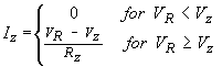 …(5)
…(5)
where
![]() represents the applied reverse
voltage as a positive quantity. These diodes are referred to as “Zener
Diodes”, but this is misleading as Zener behaviour only occurs for low
breakdown (highly doped) junctions usually ~ 5 Volts or less. Avalanche modes
dominate above this value. One additional characteristic for Avalanche operation
is that the threshold voltage increases with increasing temperature (i.e.
positive temperature coefficient). An additional (possibly) unwanted
characteristic is that the reverse voltage can contain high amounts of broad
band noise perturbations that may need to be filtered.
represents the applied reverse
voltage as a positive quantity. These diodes are referred to as “Zener
Diodes”, but this is misleading as Zener behaviour only occurs for low
breakdown (highly doped) junctions usually ~ 5 Volts or less. Avalanche modes
dominate above this value. One additional characteristic for Avalanche operation
is that the threshold voltage increases with increasing temperature (i.e.
positive temperature coefficient). An additional (possibly) unwanted
characteristic is that the reverse voltage can contain high amounts of broad
band noise perturbations that may need to be filtered.
Holes and Electrons require a certain
time to “pass through” each other at the P-N Junction. This time
![]() is called “recombination time”.
This means that there will be a corresponding time delay in a previously forward
biased diode’s ability to block current flow after it is switched into reverse
voltage. Consequently we would expect an upper frequency limit to AC to DC
rectification when
is called “recombination time”.
This means that there will be a corresponding time delay in a previously forward
biased diode’s ability to block current flow after it is switched into reverse
voltage. Consequently we would expect an upper frequency limit to AC to DC
rectification when
![]() becomes equal to one half the AC
time period, i.e.
becomes equal to one half the AC
time period, i.e.
![]() …(6)
…(6)
Current high speed PN junction diodes have “turn off” times in the order of 2 ns at moderate forward bias currents. From equation (6), the highest rectification frequency would then correspond to 250 MHz. This is not a clear-cut limit, and AC to DC power conversion efficiency will fall of at much lower frequencies. PN Junction diodes can even be shown to self-oscillate when subjected to high frequency AC signals at currents exceeding a few mA.
The effect of this charge storage is
analogous to having a current dependant capacitance placed across the junction.
The total charge
![]() stored in the junction will depend
on the forward current flowing and the time required for carrier recombination,
stored in the junction will depend
on the forward current flowing and the time required for carrier recombination,
![]() …(7)
…(7)
Since charge
![]() then we can imply a current
dependent junction capacitance of,
then we can imply a current
dependent junction capacitance of,
![]() …(8)
…(8)
As an example, a typical PN junction
diode (1N4148, BAV70 etc) will have a typical zero bias junction capacitance
< 2 pF. These also tend to display typical turn off or recombination times in
the order of
![]() . Equation (8) predicts an effective
forward biased junction capacitance of 286 pF, at a forward bias current of 100
mA, assuming a forward voltage drop of
. Equation (8) predicts an effective
forward biased junction capacitance of 286 pF, at a forward bias current of 100
mA, assuming a forward voltage drop of
![]() .
.
Certain diodes make use of this
property. PIN diodes, for example, have a thin intrinsic semiconductor layer
placed in-between the PN junction. This has the effect of inhibiting diode
rectification but allows the effective forward biased (incremental or AC)
resistance to be controlled by a forward bias current. This property is useful
in current controlled attenuation circuits. The inhibited rectification
behaviour allows large RF currents to be controlled by smaller DC forward bias
currents without distortion. Another version of the above is referred to as a
“Band Switch Diode”. The PIN diode usually has an AC resistance
![]() that closely follows,
that closely follows,
![]() …(9)
…(9)
The scale term
![]() when
when
![]() is expressed in mA. Low values of
series resistance, as might be wanted in a RF switch would require high forward
bias currents that could be unattractive. The “Band Switch Diode” attempts
to place its charge dependent capacitance in parallel with
is expressed in mA. Low values of
series resistance, as might be wanted in a RF switch would require high forward
bias currents that could be unattractive. The “Band Switch Diode” attempts
to place its charge dependent capacitance in parallel with
![]() , effectively “shorting it out”, especially at high frequencies. This allows
very low “on resistance” at bias currents around 1 mA. The two types of
diodes can be identified by their frequency behaviour. PIN diodes have a
constant
, effectively “shorting it out”, especially at high frequencies. This allows
very low “on resistance” at bias currents around 1 mA. The two types of
diodes can be identified by their frequency behaviour. PIN diodes have a
constant
![]() with frequency, whilst Band Switch
(PIN) diodes show a combined
with frequency, whilst Band Switch
(PIN) diodes show a combined
![]() that halves for each doubling in
frequency (same as a capacitor).
that halves for each doubling in
frequency (same as a capacitor).
It might be thought that temperature dependency in junction diode characteristics could be a drawback. The forward bias voltage dependency is however put to good use in temperature sensors (used to monitor a CPU core temperature, etc) and “Band Gap” voltage references used in nearly all modern voltage regulation Integrated Circuits (IC).
The variation in forward bias voltage caused by temperature in an ideal diode can be predicted from a thermally enhanced model presented in Equation (2).
 …(2 - again)
We will consider relatively low forward
bias currents where the effect of
![]() is negligible,
is negligible,
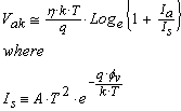 …(10)
…(10)
To further simplify the prediction we will consider the situation where the Diode anode current is significantly higher than its saturation current, which best describes normal forward biased operation, i.e.
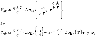 …(11)
…(11)
We will now differentiate equation (5) with respect to temperature T,
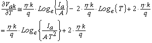 …(12)
…(12)
We observe from equation (6) that
![]() so equation (12) can be rewritten
as,
so equation (12) can be rewritten
as,
![]() …(13)
…(13)
If we assume
![]() then
then
![]() at a room temperature of
at a room temperature of
![]() . Although this value of forward voltage temperature is a useful “rule of
thumb”, it is still dependant on bias conditions and somewhat arbitrary diode
model coefficients. The main contributors involve the diode “ideality
factor”
. Although this value of forward voltage temperature is a useful “rule of
thumb”, it is still dependant on bias conditions and somewhat arbitrary diode
model coefficients. The main contributors involve the diode “ideality
factor”
![]() and the “effective barrier
height”
and the “effective barrier
height”
![]() which were anything close to ideal
or related to observable physics in the given diode data example. If actual
diode voltage temperature variation is important, it is best to consult the
actual device data directly, or failing this, to use the diode model to predict
extrapolated behaviour under actual working bias conditions.
which were anything close to ideal
or related to observable physics in the given diode data example. If actual
diode voltage temperature variation is important, it is best to consult the
actual device data directly, or failing this, to use the diode model to predict
extrapolated behaviour under actual working bias conditions.
Deriving
a Simple Figure Of Merit (FOM) For a Varicap Diode
Varicap diodes are used for electronic
tuning filters and resonators used in Voltage Controlled Oscillator (VCO). The
available frequency tuning range depends on the amount of capacitance variation
that the diode can provide, and the overall circuit Q is limited by the
parasitic series resistance term
![]() .
.
Unfortunately, the optimum choice of
diode is not clear-cut. In many applications, the available capacitance range is
far greater than required, and is “watered down” by the inclusion of a small
series capacitance
![]() .
.
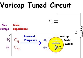
The value of series capacitance
![]() can be determined from the minimum
required resonant frequency
can be determined from the minimum
required resonant frequency
![]() , the maximum resonant frequency
, the maximum resonant frequency
![]() , the maximum Varicap diode capacitance
, the maximum Varicap diode capacitance
![]() at reverse bias voltage
at reverse bias voltage
![]() , and the minimum Varicap diode capacitance
, and the minimum Varicap diode capacitance
![]() at bias voltage
at bias voltage
![]() .
.
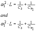 …(14)
…(14)
Eliminating
![]() and making
and making
![]() the subject,
the subject,
 …(15)
…(15)
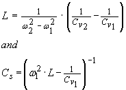
Having determined these components, we
will need to know how the Varicap diode series resistance
![]() affects the overall circuit Q. The
Varicap diode Q can be defined as,
affects the overall circuit Q. The
Varicap diode Q can be defined as,
![]() …(16)
…(16)
It can be seen that the Varicap diode
![]() reduces as the operating frequency
reduces as the operating frequency
![]() increases, or as the Varicap diode
capacitance
increases, or as the Varicap diode
capacitance
![]() increases (i.e. as the reverse bias
voltage
increases (i.e. as the reverse bias
voltage
![]() is reduced). In any given tuned
circuit, the resonant frequency is inversely proportional to the square root of
the total tuning capacitance, but the resonant frequency is directly
proportional to capacitance. The overall
is reduced). In any given tuned
circuit, the resonant frequency is inversely proportional to the square root of
the total tuning capacitance, but the resonant frequency is directly
proportional to capacitance. The overall
![]() therefore increases with resonant
frequency in a given circuit with fixed inductance. The worst case
therefore increases with resonant
frequency in a given circuit with fixed inductance. The worst case
![]() therefore occurs at the lowest bias
voltage and corresponding resonant frequency. We will define this
therefore occurs at the lowest bias
voltage and corresponding resonant frequency. We will define this
![]() condition as
condition as
![]() …(17)
…(17)
The overall minimum circuit Q also occurs at the lowest tuned frequency as,
![]() …(18)
…(18)
Substituting equation (17) and (18) into equation (15) now suggests that,
 …(19)
…(19)
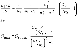
Equation (19) now provides direct
insight into a given Varicap diodes impact on the worst case circuit Q based on
the lowest tuned frequency
![]() , the relative tuning frequency range
, the relative tuning frequency range
![]() , its available tuning capacitance ratio
, its available tuning capacitance ratio
![]() and its minimum
and its minimum
![]() .
.
A suitable Varicap diode Figure of Merit
![]() can now be defined as,
can now be defined as,
![]() …(20)
…(20)
Silicon Varicap diodes have benefited
from a great deal of Research in recent years and continually push the envelope
in terms of their effective
![]() .
.
The Zener effect a quantum explanation, and tends to occur only in heavily doped diodes that exhibit high values of reverse current at reverse bias voltages less than 5 Volts. The characteristic is relatively “soft”, similar to that of a forward biased diode exponential V-I characteristic equation.
In most applications, IC based voltage references are the preferred option for accurate voltage regulation and have excellent temperature and stability. “Zener” diodes are still useful as a low cost method for clamping unwanted signal voltage “spikes”. They are also used as simple voltage references in less critical applications.
In many cases it is useful to know the incremental current and or voltage behaviour of a given component so that its small signal, low frequency characteristics can be ascertained. This analysis is usually provided for the forward bias case, with some realistic simplification.
![]() …(21) (Defined simply for the
purpose of this analysis)
…(21) (Defined simply for the
purpose of this analysis)
Differentiating with respect to voltage we find,
 …(22)
…(22)
The “dynamic conductance”
![]() is directly proportional to the
junction diode’s forward bias current
is directly proportional to the
junction diode’s forward bias current
![]() and since resistance is defined as
the reciprocal of conductance we can also state,
and since resistance is defined as
the reciprocal of conductance we can also state,
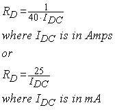
![]() …(6)
…(6)
where
![]() . The junction diode can now be seen to provide a current dependent conductance
or resistance to small signal perturbations compared to its forward bias current
. The junction diode can now be seen to provide a current dependent conductance
or resistance to small signal perturbations compared to its forward bias current
![]() . We can also gain some insight into its non- linear properties in the forward
bias region by expanding equation (4) as a Taylor series,
. We can also gain some insight into its non- linear properties in the forward
bias region by expanding equation (4) as a Taylor series,
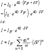 …(7)
…(7)
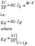
In this case
![]() represents a small perturbation in
voltage around a given forward bias voltage
represents a small perturbation in
voltage around a given forward bias voltage
![]() . Also note the n=1 tern corresponds to the previous expression for the dynamic
conductance
. Also note the n=1 tern corresponds to the previous expression for the dynamic
conductance
![]() . The n=2 term is also of interest for small signal detection and frequency
mixing. In this case
. The n=2 term is also of interest for small signal detection and frequency
mixing. In this case
![]() …(8)
…(8)
![]()
![]()
![]()
![]()
![]()
![]()
From equation (8)
![]() where
where
![]() , therefore,
, therefore,
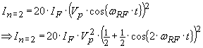 …(9)
…(9)
The average current can be found by integrating equation (9)
ignoring the cosine term and subtracting the forward bias current,
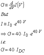 …(3), However
R = 1/G so….
…(3), However
R = 1/G so….
 …(4)
…(4)
![]()
Return to: A Component Universe
or: Ian Scotts Technology Pages
© Ian R Scott 2007 - 2008